Showing posts with label Inverters. Show all posts

Simple 100W Inverter 12VDC to 220VAC

This is Simple and Low-cost electronic circuit project for 100W inverter 12VDC to 220VAC circuit Diagram. The following diagram is an inverter circuit which will give you 220V AC 50Hz with maximum power of 100W.

100W Inverter 12VDC to 220VAC circuit diagram:

100W Inverter circuit diagram

This inverter built using transistors both the square wave generator and the amplifier.The Q1 and Q2 used generate square wave. Q5-Q8 amplify the signal and the transformer to increase the AC/square wave current from 12VAC to 220V AC 50HZ.

Inverter PCB layout:
Inverter circuit diagram


read more...

Micro Inverter circuit DC voltage AC 12v x110v

This is a micro-inverter DC voltage to AC from a 12v battery can generate a voltage of 110 or 220 volts AC and a frequency of 50Hz to 60Hz.

Micro Inverter circuit DC voltage AC 12v x110v Circuit Diagram:

Micro Inverter Circuit Diagram


The circuit is very simple and does not need a printed circuit board, It is composed of two transistors oscillators that generate the square wave pulse to the transformer in the case is 10 +10 and its output 220V or 110V. This circuit is 50Hz, but can be changed by changing the value of RC .

Inverter Circuit Diagram

This circuit has the power transistor and that depends on the transformer.


read more...

250 to 5000 watts PWM DC/AC 220V Power Inverter

Here is Simple Electronic Circuit Project of   250 to 5000 watts PWM DC/AC 220V Power Inverter Circuit Diagram.

250 to 5000 watts PWM DC/AC 220V Power Inverter

250 to 5000 watts PWM DC/AC 220V Power Inverter


DC/AC 220V Power Inverter

This is my schematic design of a Pulse Width Modulator DC/AC inverter using the chip SG3524 .
I have built this design and using it as a backup to power up all my house when outages occur.

250 to 5000 watts PWM DC/AC 220V Power Inverter

https://blogger.googleusercontent.com/img/b/R29vZ2xl/AVvXsEj27B09k4PtSZsekIonNLpkjrsbjpxa5_LDkju8yjmh-SnmD5IQKMsNEu60vOgNE_ielw7_PtMmsvFByTmM1S-_VPiFo6HcaEAi7Fqyntd91wc0N7G_3SiRENb_4h6eJfC5XSwDqNdVmek/s1600/250+to+5000+watts+PWM+DC-AC+220V+Power+Inverter5.jpg

220V Power Inverter


If you like my work and intend to build the circuit don't forget to give me the 5 satrs :D and subscribe to me by clicking on the "follow" button so I know how many people benefit from the design, Thanks

DC/AC 220V Power Inverter

250 to 5000 watts PWM DC/AC 220V Power Inverter

250 to 5000 watts Inverter

250 to 5000 watts

https://blogger.googleusercontent.com/img/b/R29vZ2xl/AVvXsEjMRrNxdulo80zGWhUQ-H3VCXR3lepourIaGDHzMNqo05S584Yd91T_rdSZmmrTTm7FSrEqEj_EOvPMu_gkaBVVhOHPg2dIDVw3wS0q0Da1axeoOpgLm03ImbMk4CmysG2zOmcbSaFIsOc/s1600/250+to+5000+watts+PWM+DC-AC+220V+Power+Inverter+10.jpg

220V Power Inverter

watts PWM DC/AC 220V Power Inverter

PWM DC/AC 220V Power Inverter


Notes:

>The schematic circuit design is for a 250 watt output, while the pics are of my 1500 watts inverter that i built, to increase the power of the circuit you have to add more of the Q7 and Q8 transistors in parallel, each pair you add will increase your power by 250 watts, ex: to get 750 watts of power from the inverter you need to add in parallel 2 of Q7 and 2 of Q8 to the original design.

>If you increase the power transistors you have to enlarge the T2 transformer to match the new needs, the circuit's transformer is rated 25 amps to handle 250 watts of 220v, for every 1 additional amp you need on the 220v side you have to increase 10 amps on the 12v side, of course there are limits to the thickness of the winding so if you need more than 750 watts i recommend that you use a 24VDC supply instead of 12 volts:

DC voltage and Transformer "T2" winding recommendation:
Power     Supply     Winding
750w       12VDC     P:24V "12-0-12" / S:220V
1500w     24VDC     P:48V "24-0-24" / S:220V
2250w     36VDC     P:72V "36-0-36" / S:220V
3000w     48VDC     P:96V "48-0-48" / S:220V
3750w     60VDC     P:120V "60-0-60" / S:220V
4500w     72VDC     P:144V "72-0-72" / S:220V
5250w     84VDC     P:168V "84-0-84" / S:220V
*The transformer should be "center tapped" at the primary side.
**You can make the secondary 110v if needed.
***The transformer in the pic is a custom made (48V center tapped / 220v ) 2000 watts, weights like 10 kilos.

>R1 is to set the PWM duty cycle to 220v. Connect voltmeter to the output of your inverter and vary VR1 till the voltage reads 220V.

>R2 is to set the frequency to 50 or 60 Hz (R2 range is between 40Hz to 75Hz), so guys that do not have a frequency meter are advised to blindly put this variable resistor mid-way which should drop you in the range of 50~60 Hz.
If you want you can substitue the variable resistor with a fixed resistor using the following formula: F = 1.3 / (RxC)
in our case to get a 50Hz output we remove both the 100K and the variable 100K both from pin 6 and we put instead a 260K fixed resistor and we leave the 0.1uF (the 104 cap) as it is, this change should give out a fixed 50Hz as per the formula :
1.3 / (260,000 ohm x 0.0000001 farad) = 50Hz
But in reality it will not exactly give 50Hz because the 260K resistor has a specific error value margin so does the capacitor, that's why i recommend a variable resistor so that accurate calibration can be achieved.

>Use either tantalum or polyester film "as in pic" for the 104 caps, ceramic disc caps change value once hot and this in turn changes the frequency of the inverter so they are not recommended.

>Pin 10 of the SG3524 can be used to auto shut down the inverter, once a positive voltage is given instead of negative to pin10, the SG3524 will stop oscillating. This is useful for persons wanting to add some cosmetic makeup to their inverters like overload cutoff, low battery cutoff or overheating cutoff.

>Wiring connections on the power stage side should be thick enough to handle the huge amps drain from the batteries. I marked them with dark black on the schema also I included a pic so you see how thick those wires must be.

>The design does not include a battery charger since each person will be building a custom version of the inverter with specific power needs. If you are ordering a custom made transformer you can ask them to take out for you an additional output wire on the primary side to give 14v (between point 0 and this new wire) and use it to charge a 12v battery, of course this needs a seperate circuit to control charging auto cut-off. But anyway this is not advisable because it will shorten the life of the transformer itself since using it as a charger will toast the enamel coating layer of the copper wires over time. Anyway .. YES can be done to reduce cost.

>A cooling fan will be needed to reduce heat off the heat sinks and transformer, i recommend getting a 220v fan and connecting it to the output T2 transformer, when you power up the circuit the fan will start this will always give you a simple way to know that 220v is present and everything is OK.. You can use a computer's old power supply fan if you like.
Note that the fan must suck air out from the inverter case and NOT blow inside, so install it the correct way or it will be useless.
Also note how I fixed both the heat sinks and where the fan is, in a way that the fan sucks hot air from like a channel between the 2 heatsinks.

>2 circuit breakers are recommended instead of fuses, one on the DC side and one on the AC side, depending on your design
Ex: for a 24vDC ( 1500 watts design ) put a 60Amp breaker on the DC side and a 6Amp on the AC side.
For every 1amp of 220vAC you will be draining like 8 to 10 Amps from the 12v battery, make your calculations !

> The 2 Heat sinks should be big enough to cool the transistors, they are separate and should NOT touch each other. "see the pics"

>Important: If you're building a big design that uses more than 24VDC as power source, make sure not to supply the driver circuit with more than 24v maximum. (EX: If you have 4 batteries 4x12 = 48v , connect the v+ supply of the driver circuit to the second battery's (+) terminal with a thin 1 mm wire which is more than enough. this supplies the driver circuit with +24v while supplies the power transformer with +48v)

> "Optional" : Deep Cycle batteries are your best choice, consider them for best results .. read more

> Be cautious when building this circuit it involves high voltage which is lethal, any part you touch when the circuit is ON could give you a nasty painful jolt, specially the heat-sinks, never touch them when the circuit is on to see if the transistors are hot !! I ate it several times :)

> The optional "Low voltage warning" is already embedded in the PCB layout, you can disregard it and not install it's components if you do not needed. It does not affect the functionality of the main circuit.

> The Motorola 2N6277 is a heavy duty power transistor, it is used in many US tanks for it's reliability but unfortunately it is a very hard to find part, instead you can substitute each 2N6277 with 2 x 2N3773 or any equivalent.

> I've included an optional "Battery level indicator" circuit diagram that has 4 LEDs, you can see it installed on the front panel of my inverter pic, it is functioning great and shows precisely how much juice the batteries still have. I have included a small relay that is powered by the last LED to auto shutoff the inverter once last LED is off.

>Also included an optional "Overload circuit", it is very easy to build and can be calibrated to the desired overload current threshold cutoff point through the potentiometer VR1.

R1 is rated 5watts for inverters upto 1000 watts. For bigger versions of the inverter like 1000 to 3000 watts inverters, replace R1 (1 ohm, 5watts) with (1 ohm, 17watts) which should handle loads upto 10 VA.
Make sure you install a proper relay to handle big current drains.

 If you like my work; you can show your regards by hitting Facebook like button, following us on Google+ or Twitter, stumbling our posts on stumble upon . Stay tuned for more tech updates.

read more...

Simple Portable Power Inverter

Recently, my neighbor expressed a deep interest in building a low-power inverter from scratch. This portable power inverter takes the dc output from a low-voltage accumulator and creates a stable 230-VAC/50-Hz mains suitable for powering small items of equipment. As several inverter designs have already been published on the web, the goal here was to make the design easily accessible to others by using familiar and easily sourced components available to novices and hobbyists everywhere. Here is the design that uses readily obtainable N-type FETS and an inexpensive CMOS chip to generate the square wave signals. Because the square wave signals are generated by a single chip, it can easily be modified for 50 Hz or 60 Hz, either 115 V or 230 V, and a broad range of input voltages. 

Portable Power Inverter Circuit Diagram:

Inverter Circuit Diagram

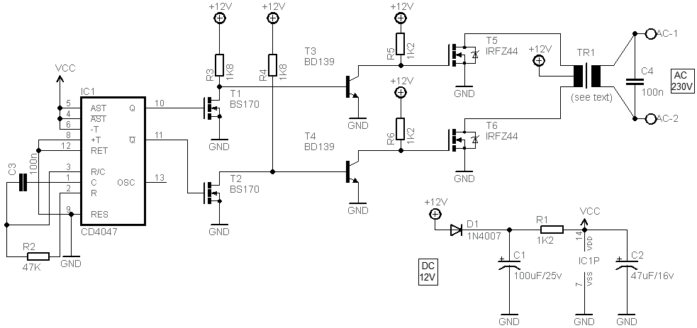
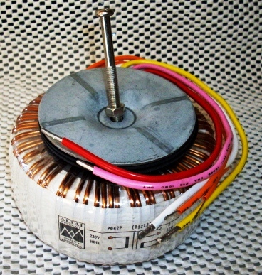
The circuit is built around the monostable/astable multivibrator CD4047 (IC1). The resistor (R2) and capacitor (C3), connected to pins 2 and 3, will decide the frequency of the astable output pulses (here, it is at about 50 Hz). IC1 gives two similar frequency outputs at pins 10 and 11 (phase of the Q and Q signals varies about 180 degrees). The square wave output signals are processed by the two-channel transistor banks (T1-T3-T5 and T2-T4-T6) to drive the power transformer (TR1). In my prototype, TR1 is a 60-VA toroidal transformer with a nominal 12-V rms secondary and 5-A current. I have powered up the inverter with an SMF battery of 12 V close to 7 Ah and successfully powered one 230-V/40-W lightbulb. The efficiency looks promising with neither the MOSFETs nor the transformer getting hotter than warm.


Power Inverter Circuit DiagramPortable Circuit Diagram

Parts List:
 
IC1: CD4047N
T1, T2: BS170
T3, T4: BD139 (or D400)
T5, T6: IRFZ44N
D1: 1N4007
C1: 100 uF/25 V
C2: 47 uF/16 V
C3: 100 nF/63 V
C4: 100 nF/400 V~
R1: 1K2
R2: 47K (change to 39K for 60 Hz)
R3, R4: 1K8
R5, R6: 1K2
TR1: (see text)

Power Circuit Diagram

Because the inverter has fatal mains voltages present, it is highly recommended that it be put into a metal enclosure (with adequate vent holes). The largest component is the toroidal transformer, which should be securely mounted to the chassis. A proper (TO-220) heatsink should be used with the FETs (T5-T6). Note that both the upper and lower FETs can be bolted into a single (TO220x2) heatsink plate, provided that they are insulated from each other and from the heatsink plate. The proposed portable power inverter is intended to be used when there is no option to use ac mains for certain low-wattage devices (for example, as an in-car/camping inverter). I am happy to receive feedback from readers in the hope that this primitive design will evolve into an efficient unit!

Author By: T.K. HAREENDRAN


read more...

12V Power Inverter using 555 Timer

This 12V power inverter circuit is very useful when you want to use a 240 volts consumer powered by a 12 volts car battery .In contrast to the usual feedback oscillator type of inverter, the oscillator of this inverter use a 555 timer connected as an astable multivibrator that is separate from the output stage, which allows easy adjustment of the oscillator frequency to suit different applications.

This 12V power inverter circuit can be used to power small power devices that need a 240 volts .

12V Power Inverter using 555 Timer Circuit Diagram:

12V Power Inverter

The output of the 555 timer drives the base of T1 and T2 transistors . The wattage of this 12 volts inverter circuit depend on the driver transistors and the output transformer used . The output of this circuit will provide a 240v at 50Hz.

read more...

1KVA (1000 watts) Pure Sine Wave Inverter

As can be seen in the first diagram below, the configuration is a simple mosfet based designed for amplifying current at +/-60 volts such that the connected transformer corresponds to generate the required 1kva output. Q1, Q2 forms the initial differential amplifier stage which appropriately raises the 1vpp sine signal at its input to a level which becomes suitable for initiating the driver stage made up of Q3, Q4, Q5.

1KVA (1000 watts) Pure Sine Wave Inverter Circuit Diagram:

Inverter Circuit Diagram

The mosfets are also formed in the push pull format, which effectively shuffles the entire 60 volts across the transformer windings 50 times per second such that the output of the transformer generates the intended 1000 watts AC at the mains level. For acquiring the intended pure sine wave output, a suitable sine input is required which is fulfilled with the help of a simple sine wave generator circuit. It is made up of a couple of opamps and a few other passive parts.

It must be operated with voltages between 5 and 12. This voltage should be suitably derived from one of the batteries which are being incorporated for driving the inverter circuit. The below given diagram shows a simple sine wave generator circuit which may be used for driving the above inverter circuit, however since the output from this generator is exponential by nature, might cause a lot of heating of the mosfets. A better option would be to incorporate a PWM based circuit which would supply the above circuit with appropriately optimized PWM pulses equivalent to a standard sine signal.

read more...

Electronic Router UPS

This is a simple Electronic Router UPS Circuit Diagram Project. It can be handy to have your phone and Internet router continue working for a while after  a power failure for example, if they provide  access to a security system. This requires a  backup power supply for the router. The version described here consists of a 12-V lead-acid battery and a voltage converter capable  of supplying an output voltage in the range of  15 to 30 V. It has built-in protection to prevent  excessive battery discharge.  This is uninterruptible power supply (UPS)  operates in standby mode as long as the  mains voltage is present.

Router UPS Circuit Diagram:

Electronic Router UPS

The UPS consists of four parts: a backup  detector circuit that monitors the supply  voltage from the AC mains adapter, a battery  circuit that monitors the battery voltage to  prevent it from dropping below 11.8 V, a FET  switch between the battery and the voltage  converter, and a voltage doubler (inside the  dashed outline). To understand how it works, first consider  the situation with a router supply voltage  above 20 V, for which the voltage doubler is  not required. In this case the outputs of com-parators IC1a and IC1b (pins 1 and 7) are connected directly to the gate of the FET (G1 is  connected to G2).

Under normal conditions the router, which is  connected to K3, is powered from the voltage  on connector K1. In this situation the voltage  on pin 2 of comparator IC1a is higher than 5.6  V. The output on pin 1 is therefore low, and  the FET is switched off. If the external volt-age on K1 drops out, the voltage on pin 2 of  IC1 drops and the output on pin 1 goes high,  switching on the FET. In this state the battery and the voltage converter supply power  to the router. The battery will gradually discharge, and to prevent the battery voltage  from dropping below 11.8 V the output of  the second comparator (on pin 7) goes low  when the voltage reaches this threshold level,  switching off the FET. The battery voltage  may rise quickly after the FET is switched off, so capacitor C3 is included to ensure that this  does not cause the FET be switched on again.

Switch S1 allows the UPS to start up without an external supply voltage on K1, and capacitor C4 enables the comparators to continue operating in the event of a brief dropout of  the two supply voltages on K1 and K2. The emergency stop switch S2 and fuse F1 are included for safety reasons. The voltage converter has a high inrush current, so F1 must be generously dimensioned.

If the router supply voltage is below 19 V, the  comparator output level in the high state is  too low to achieve a gate–source voltage of  4.5 to 5 V, since the source voltage is always  the same as the battery voltage under continuous charging, which is 13.8 V. This means  that the gate voltage must be at least 18.3 to  18.8 V, which is difficult or impossible with a  router supply voltage under 19 V. This can be  remedied by including the voltage doubler,  which is built around the well-known 555  timer IC (CMOS version). The frequency of the  oscillator (IC2) is approximately 40 kHz. Components C6, D5 and D6 add the AC voltage to  the switched supply voltage delivered by T2,  which is driven by the comparators in parallel  with the timer reset. An 18-V Zener diode (C7)  protects the FET gate–source junction against  overvoltage.

Be careful to select a 555 with a maximum  rated supply voltage sufficient for this application; they are available in 16-V and 18-V  versions. The voltage converter of this UPS is a note-book power converter designed for in-car  use, with an input voltage of 12 V, selectable output voltage, and a minimum current  capacity of 0.5 A. Most voltage converters can  handle this easily. The battery must be connected to a good charger capable of maintaining a lead-acid battery in good condition  under prolonged no-load operation. Various  designs for this have been described in Elektor in the past.

Adjust P1 for a voltage of approximately 7 V. With a lab power supply connected in place of the battery, adjust P2 for a threshold volt-age of 11.8 V.


read more...

Micro Inverter circuit DC voltage AC 12v x110v

This is a micro-inverter DC voltage to AC from a 12v battery can generate a voltage of 110 or 220 volts AC and a frequency of 50Hz to 60Hz.

Micro Inverter circuit DC voltage AC 12v x110v Circuit Diagram:

Micro Inverter

The circuit is very simple and does not need a printed circuit board, It is composed of two transistors oscillators that generate the square wave pulse to the transformer in the case is 10 +10 and its output 220V or 110V. This circuit is 50Hz, but can be changed by changing the value of RC .


This circuit has the power transistor and that depends on the transformer.


Micro Inverter circuit DC voltage AC 12v x110v Circuit Diagram


read more...

DC to AC Inverter with 555

This circuit is more of a DC to AC inverter, it uses a 555 IC as a low frequency oscillator, adjustable, adjustment can be done by the potentiometer R4 and frequency should be between 50-60 Hertz.

DC to AC Inverter with 555 Circuit Diagram:

DC to AC Inverter with 555 Circuit Diagram


The pulses from the IC 555 will go to Q1 and Q2 are amplified and sent to the transformer T1, which has its winding reversed. Capacitor C4 and coil L1 filter are the input to T1, it effectively ensures that a sine wave is formed.

List of components:

R1 = 10K
R2 = 100K
R3 = 100 ohms
R4 = 50K potmeter
C1, C2 = 0.1μF
C3 = 0.01μF
C4 = 2700μF
Q1 = TIP41A, NTE196, ECG196
Q2 = TIP42A, NTE197, ECG197
L1 = 1μH
T1 = Transformer


read more...

100W Inverter 12VDC to 220VAC

This is a Simple electronic circuit Project of 100W Inverter 12VDC to 220VAC circuit diagram. The following diagram is an inverter circuit which will give you 220V AC 50Hz with maximum power of 100W.

100W Inverter 12VDC to 220VAC circuit diagram:

100W Inverter

Inverter PCB layout:

100W Inverter 12VDC to 220VAC


This inverter built using transistors both the square wave generator and the amplifier.The Q1 and Q2 used generate square wave. Q5-Q8 amplify the signal and the transformer to increase the AC/square wave current from 12VAC to 220V AC 50HZ.
read more...

Build A UPS Power Supply

This circuit is a simple form of the commercial UPS, the circuit provides a constant regulated 5 Volt output and an unregulated 12 Volt supply. In the event of electrical supply line failure the battery takes over, with no spikes on the regulated supply.

UPS

This circuit can be adapted for other regulated and unregulated voltages by using different regulators and batteries. For a 15 Volt regulated supply use two 12 Volt batteries in series and a 7815 regulator. There is a lot of flexibility in this circuit.

TR1 has a primary matched to the local electrical supply which is 240 Volts in the UK. The secondary winding should be rated at least 12 Volts at 2 amp, but can be higher, for example 15 Volts. FS1 is a slow blow type and protects against short circuits on the output, or indeed a faulty cell in a rechargeable battery. LED 1 will light ONLY when the electricity supply is present, with a power failure the LED will go out and output voltage is maintained by the battery. The circuit below simulates a working circuit with mains power applied:
Power Supply

Between terminals VP1 and VP3 the nominal unregulated supply is available and a 5 Volt regulated supply between VP1 and VP2. Resistor R1 and D1 are the charging path for battery B1. D1 and D3 prevent LED1 being illuminated under power fail conditions. The battery is designed to be trickle charged, charging current defined as :-

(VP5 - 0.6 ) / R1
where VP5 is the unregulated DC power supply voltage.

D2 must be included in the circuit, without D2 the battery would charge from the full supply voltage without current limit, which would cause damage and overheating of some rechargeable batteries. An electrical power outage is simulated below:

Circuit Diagram for UPS

Note that in all cases the 5 Volt regulated supply is maintained constantly, whilst the unregulated supply will vary a few volts.

Standby Capacity
The ability to maintain the regulated supply with no electrical supply depends on the load taken from the UPS and also the Ampere hour capacity of the battery. If you were using a 7A/h 12 Volt battery and load from the 5 Volt regulator was 0.5 Amp (and no load from the unregulated supply) then the regulated supply would be maintained for around 14 hours. Greater A/h capacity batteries would provide a longer standby time, and vice versa.
read more...

Simple and Small Power Inverter

Even robot systems occasionally need a negative supply voltage for some purpose or other, and in this kind of application in particular there is a need for an effective circuit that does  not  make  greater demands  then  necessary in terms of current or space. If a low current 5 V supply is needed and only +5 V is available, a natural manufacturer to turn  to  is  Maxim,  and indeed in this case they do not let us down.The best known integrated  circuit made by this company is the MAX232, a level shifter for serial ports with an integrated charge pump that does not need an external inductor.

Simple Mini Power Inverter image:

Inverter image

Along the same lines, although with a more stable output voltage and higher efficiency, is the MAX660. The device can ‘mirror’ any input voltage between 1.5 V and 5.5 V. With a 5 V input the output is typically –4.7 V with a load of 100 mA. Efficiency at 10 mA is around 96 % and at 100 mA is around 88 %. With an open-circuit output the IC draws a quiescent current of just 120 μA.There is little to say about the circuit itself.

Simple Mini Power Inverter Circuit diagram:

Inverter Circuit diagram
 
The 0 Ω resistor on pin 1 selects the operating frequency. With R1 fitted, the circuit operates at 80 kHz; without it, at 10 kHz. The combination of L1 and C5 slightly reduces ripple on the output voltage; the choice of inductor is not as critical as it would be if it formed part of the switching circuit.Gerber files for the printed circuit board (which uses some SMD components) are available for download from the Elektor website, ref. 070279-11.zip. R1, C1 and C4 are 0603 SMDs and C3 is an SMD tantalum electrolytic capacitor. Either the MAX-660CSA or the MAX660M can be used; both come in SO8 packages. L1 is a 10 μH SMD inductor rated at 300 mA. Source Link: Circuits-Projects

 
read more...

Simple Cheap 12V to 220V Inverter

Even though today’s electrical appliances are increasingly often self-powered, especially the portable ones you carry around when camping or holidaying in summer, you do still sometimes need a source of 230 V AC - and while we’re about it, why not at a frequency close to that of the mains? As long as the power required from such a source remains relatively low - here we’ve chosen 30 VA - it’s very easy to build an inverter with simple, cheap components that many electronics hobbyists may even already have.

Though it is possible to build a more powerful circuit, the complexity caused by the very heavy currents to be handled on the low-voltage side leads to circuits that would be out of place in this summer issue. Let’s not forget, for example, that just to get a meager 1 amp at 230 VAC, the battery primary side would have to handle more than 20 ADC!. The circuit diagram of our project is easy to follow. A classic 555 timer chip, identified as IC1, is configured as an astable multivibrator at a frequency close to 100 Hz, which can be adjusted accurately by means of potentiometer P1.

Cheap 12V to 220V Inverter Circuit Diagram:

Inverter
 
As the mark/space ratio (duty factor) of the 555 output is a long way from being 1:1 (50%), it is used to drive a D-type flip-flop produced using a CMOS type 4013 IC. This produces perfect complementary square-wave signals (i.e. in antiphase) on its Q and Q outputs suitable for driving the output power transistors. As the output current available from the CMOS 4013 is very small, Darlington power transistors are used to arrive at the necessary output current. We have chosen MJ3001s from the now defunct Motorola (only as a semi-conductor manufacturer, of course!) which are cheap and readily available, but any equivalent power Darlington could be used.

These drive a 230 V to 2 × 9 V center-tapped transformer used ‘backwards’ to produce the 230 V output. The presence of the 230 VAC voltage is indicated by a neon light, while a VDR (voltage dependent resistor) type S10K250 or S07K250 clips off the spikes and surges that may appear at the transistor switching points. The output signal this circuit produces is approximately a square wave; only approximately, since it is somewhat distorted by passing through the transformer. Fortunately, it is suitable for the majority of electrical devices it is capable of supplying, whether they be light bulbs, small motors, or power supplies for electronic devices.

PCB layout:
invertor-circuit-diagram


Parts List :

Resistors
R1 = 18k?
R2 = 3k3
R3 = 1k
R4,R5 = 1k?5
R6 = VDR S10K250 (or S07K250)
P1 = 100 k potentiometer
Capacitors
C1 = 330nF
C2 = 1000 µF 25V
Semiconductor
T1,T2 = MJ3001
IC1 = 555
IC2 = 4013
Miscellaneous
LA1 = neon light 230 V
F1 = fuse, 5A
TR1 = mains transformer, 2x9V 40VA (see text)
4 solder pins

Note that, even though the circuit is intended and designed for powering by a car battery, i.e. from 12 V, the transformer is specified with a 9 V primary. But at full power you need to allow for a voltage drop of around 3 V between the collector and emitter of the power transistors. This relatively high saturation voltage is in fact a ‘shortcoming’ common to all devices in Darlington configuration, which actually consists of two transistors in one case. We’re suggesting a PCB design to make it easy to construct this project; as the component overlay shows, the PCB only carries the low-power, low-voltage components.

The Darlington transistors should be fitted onto a finned anodized aluminum heat-sink using the standard insulating accessories of mica washers and shouldered washers, as their collectors are connected to the metal cans and would otherwise be short-circuited. An output power of 30 VA implies a current consumption of the order of 3 A from the 12 V battery at the ‘primary side’. So the wires connecting the collectors of the MJ3001s [1] T1 and T2 to the transformer primary, the emitters of T1 and T2 to the battery negative terminal, and the battery positive terminal to the transformer primary will need to have a minimum cross-sectional area of 2 mm2 so as to minimize voltage drop.

The transformer can be any 230 V to 2 × 9 V type, with an E/I iron core or toroidal, rated at around 40 VA. Properly constructed on the board shown here, the circuit should work at once, the only adjustment being to set the output to a frequency of 50 Hz with P1. You should keep in minds that the frequency stability of the 555 is fairly poor by today’s standards, so you shouldn’t rely on it to drive your radio-alarm correctly – but is such a device very useful or indeed desirable to have on holiday anyway? Watch out too for the fact that the output voltage of this inverter is just as dangerous as the mains from your domestic power sockets.

So you need to apply just the same safety rules! Also, the project should be enclosed in a sturdy ABS or diecast so no parts can be touched while in operation. The circuit should not be too difficult to adapt to other mains voltages or frequencies, for example 110 V, 115 V or 127 V, 60 Hz. The AC voltage requires a transformer with a different primary voltage (which here becomes the secondary), and the frequency, some adjusting of P1 and possibly minor changes to the values of timing components R1 and C1 on the 555.

read more...

Low- Cost Power Mosfet Inverter

This is simple and Low-cost circuit diagram project of simple power mosfet inverter circuit. This inverter can deliver .high-voltage ac or de, with a rectifier and filter, up to several hundred volts.

Low- Cost Power Mosfet Inverter Circuit Diagram:

Inverter Circuit Diagram

The secondary and primary of T1-a 12.6 to 440 V power transformer, respectively-are reversed; e.g., the primary becomes the secondary and the secondary becomes the primary. Transistors Q1 and Q2 can be any power FET.

Note:
Be sure to heat sink Q1 and Q2. Capacitors C1 and C2 are used as spike suppressors.

read more...

Low-cost Power Inverter

Here is simple but low-cost power inverter circuit project. This power inerter any transformer can be use 6.3 or 12.6 V type.

Low-cost Power Inverter Circuit Diagram:

Low-cost Power Inverter

Apply the 12-Vde input so the positive goes to the transformer`s center tap and the negative goes to the two transistor emitters. Any bridge type rectifier and filter can be used at the output, if you need de.

read more...

Simple Power Mosfet Inverter

This a very simple Electronic Circuit Project of Power Mosfet Inverter Circuit Diagram. This inverter can deliver .high-voltage ac or de, with a rectifier and filter, up to several hundred volts.

Inverter

The secondary and primary of T1-a 12.6 to 440 V power transformer, respectively-are reversed; e.g., the primary becomes the secondary and the secondary becomes the primary. Transistors Q1 and Q2 can be any power FET.

Be sure to heat sink Q1 and Q2. Capacitors C1 and C2 are used as spike suppressors.

read more...

DC to AC Inverter Using 555 Timer

Here is a Electronic Circuit Project of DC to AC Inverter circuit. This DC-to-AC inverter schematic produces an AC output at line frequency and voltage. The 555 is configured as a low-frequency oscillator, tunable over the frequency range of 50 to 60 Hz by Frequency potentiometer R4.

The 555 feeds its output (amplified by Q1 and Q2) to the input of transformer T1, a reverse-connected filament transformer with the necessary step-up turns ratio. Capacitor C4 and coil L1 filter the input to T1, assuring that it is effectively a sine wave. Adjust the value of T1 to your voltage.

DC to AC Inverter Circuit Diagram:

DC to AC Inverter Circuit Diagram

The output (in watts) is up to you by selecting different components.

Input voltage is anywhere from +5V to +15Volt DC, adjust the 2700uF cap's working voltage accordingly.
Replacement types for Q1 are: TIP41B, TIP41C, NTE196, ECG196, etc. Replacement types for Q2 are: TIP42B, TIP42C, NTE197, ECG197, etc. Don't be afraid to use another type of similar specs, it's only a transistor... ;-)


If the whole thing is working, good. If not, relax and don't get frustrated. Do the following checks:
  1. You have connected the filament transformer in REVERSE yes?
  2. If not, disconnect the power and reverse. If you have, disconnect the transformer and measure the voltage after L1 and ground.
  3. Just in case, GROUND for this circuit is same as negative (-).
  4. Q1/Q2 are oposites, e.i. npn/pnp.
  5. Is your 555 perhaps defective? Disconnect R3 from pin 3 and check pin 3 for a pulse.
  6. Check your transistors to make sure they are not defective.
Error fix: Pin 7 and 2 were reversed. Original pinout was correct.

Parts List:
   R1 = 10K
   R2 = 100K
   R3 = 100 ohm
   R4 = 50K potmeter, Linear
C1,C2 = 0.1uF
   C3 = 0.01uF
   C4 = 2700uF
   Q1 = TIP41A, NPN, or equivalent transistor
   Q2 = TIP42A, PNP, or equivalent transistor
   L1 = 1uH
   T1 = Filament transformer, your choice


read more...

Electronic Project 500W Low-cost 12V to 220V inverter


This Electronic Inverter Project low-cost and very simple build 500W low-cost 12V to 220V inverter circuit project. Using this circuit you can convert the 12V dc in to the 220V Ac. In this circuit 4047 is use to generate the square wave of 50hz and amplify the current and then amplify the voltage by using the step transformer.

12V to 220V inverter Circuit Diagram:

inverter Circuit Diagram

How to calculate transformer rating:

  • The basic formula is P=VI and between input output of the transformer we have Power input = Power output
  • For example if we want a 220W output at 220V then we need 1A at the output. Then at the input we must have at least 18.3V at 12V because: 12V*18.3 = 220v*1
  • So you have to wind the step up transformer 12v to 220v but input winding must be capable to bear 20A.

read more...

Small and Super Inverter

Here is a small and super inverter circuit project. This circuit can be used to power a small strobe or fluorescent lamp. It will generate over 400 VDC from a 12 VDC, 2.5 A power supply or an auto or marine battery. While size, weight, and efficiency are nothing to write home about - in fact, they are quite pitiful - all components are readily available (even from Radio Shack) and construction is very straightforward. No custom coils or transformers are required. If wired correctly, it will work.

Output depends on input voltage. Adjust for your application. With the component values given, it will generate over 400 V from a 12 V supply and charge a 200 uF capacitor to 300 V in under 5 seconds.

Super Inverter Circuit Diagram:

Inverter Circuit Diagram


For your less intense applications, a fluorescent lamp can be powered directly from the secondary (without any other components). This works reasonably well with a F13-T5 or F15-T12 bulb (but don't expect super brightness). Q1 does get quite hot so use a good heat sink.

Notes:
  • Construction can take any convenient form - perf board, minibox, etc. Make sure the output connections are well insulated.
  • C1 must be nonpolarized type - not an electrolytic.
  • D1 provides a return path for the base drive and prevents significant reverse voltage on the B-E junction. Any 1 A or greater silicon diode should be fine.
  • C2 is shown as typical energy storage capacitor for strobe applications. Remove D2 and C2 for use with a fluorescent lamps.
  • D2 should be a high speed (fast recovery) rectifier. However, for testing, a 1N4007 should work well enough. R2 limits surge current through D2.
  • The polarity of the input with respect to the output leads is important. Select for maximum voltage by interchanging the black output wires.
  • Mount Q1 (2N3055) on a heat sink if continuous operation is desired. It will get warm. Other NPN power transistors with Vceo > 80 V, Ic > 2 A, and Hfe > 15 should work. For a PNP type, reverse the the polarities of the power supply and D1, and interchange one set of leads (where a diode is used for DC output).
  • Some experimentation with component values may improve performance for your application.
  • When testing, use a variable power supply so you get a feel for how much output voltage is produced for each input voltage. Component values are not critical but behavior under varying input/output voltage and load conditions will be affected by R1 and C1 (and the gain of your particular transistor).

WARNING:
Output is high voltage and dangerous even without large energy storage capacitor. With one, it can be lethal. Take appropriate precautions. 

Inverter Circuit Diagram


read more...

Electronic Circuit Project of DC-DC Regulating Converter

Here is a simple Electronic Circuit Project of  DC-DC regulating converter circuit. Push-pull outputs are used in this transformer-coupled dc-dc regulating converter.

DC-DC Regulating Converter Circuit Diagram:

Electronic Circuit Project of

Note that the oscillator must be set at twice the desired output frequency as the SGI 524`s internal flip-flop divides the frequency by 2 as it switches the PWM signal from one output to the other Current limiting is done here in the primary so that the pulse width will be reduced should transformer saturation occur.


read more...
 
Copyright © 2019 W3circuits.blogspot.com • All Rights Reserved.
back to top