Showing posts with label Power Supply. Show all posts

0-50V 2A Bench power supply

An 0-50v bench power supply can be made using electronic diagram below which is designed using LM10 op amp and 2n3055 transistors.

50V Bench Power Supply Circuit Diagram:

0-50V 2A Bench power supply

This LM10 2n3055 50v bench power supply allows an output voltage regulation in a range between 0 and 50 volts and the output current can be limited to a maximum of 2A. Output voltage increases linearly with the amount of resistance potentiometer P1, while the current can be adjusted linear using potentiometer P3. Potentiometer P2 serves to regulate maximum output current (maximum value is 2A).
read more...

Transformerless 5 Volt DC Power Supply

An increasing number of appliances draw a very small current from the power supply. If you need to design a mains-powered device, you could generally choose between a linear and a switch-mode power supply. However, what if the appliance’s total power consumption is very small? Transformer-based power supplies are bulky, while the switchers are generally made to provide greater current output, with a significant increase in complexity, problems involving PCB layout and, inherently, reduced reliability.

Is it possible to create a simple, minimum part-count mains (230 VAC primary) power supply, without transformers or coils, capable of delivering about 100mA at, say, 5 V? A general approach could be to employ a highly inefficient stabilizer that would rectify AC and, utilizing a zener diode to provide a 5.1 V output, dissipate all the excess from 5.1 V to (230×√2) volts in a resistor. Even if the load would require only about 10mA, the loss would be approximately 3 watts, so a significant heat dissipation would occur even for such a small power consumption.


Transformerless 5 Volt DC Power Supply Circuit Diagram:


Power Supply Circuit Diagram
 
At 100mA, the useless dissipation would go over 30 W, making this scheme completely unacceptable. Power conversion efficiency is not a major consideration here; instead, the basic problem is how to reduce heavy dissipation and protect the components from burning out. The circuit shown here is one of the simplest ways to achieve the above goals in practice. A JVR varistor is used for over-voltage/surge protection. Voltage divider R1-R2 follows the rectified 230 V and, when it is high enough, T1 turns on and T3 cannot conduct.

When the rectified voltage drops, T1 turns off and T3 starts to conduct current into the reservoir capacitor C1. The interception point (the moment when T1 turns off) is set by P1 (usually set to about 3k3), which controls the total output current capacity of the power supply: reducing P1 makes T1 react later, stopping T3 later, so more current is supplied, but with increased heat dissipation. Components T2, R3 and C2 form a typical ‘soft start’ circuit to reduce current spikes — this is necessary in order to limit C1’s charging current when the power supply is initially turned on. At a given setting of P1, the output current through R5 is constant.

Thus, load R4 takes as much current as it requires, while the rest goes through a zener diode, D5. Knowing the maximum current drawn by the load allows adjusting P1 to such a value as to provide a total current through R5 just 5 to 6mA over the maximum required by the load. In this way, unnecessary dissipation is much reduced, with zener stabilization function preserved. Zener diode D5 also protects C1 from over voltages, thus enabling te use of low-cost 16 V electrolytics. The current flow through R5 and D5, even when the load is disconnected, prevents T3’s gate-source voltage from rising too much and causing damage to device. In addition, T1 need not be a high-voltage transistor, but its current gain should exceed 120 (e.g. BC546B, or even BC547C can be used).


read more...

Simple Uninterrupted Power Supply

The Uninterrupted Power Supply in an IC . Cymbet Corporation announced the availability of the EnerChip™ CC CBC3105 smart solid state battery. The CBC3105 combines the award winning EnerChip battery with integrated input power conversion, battery management and regulated output capabilities. The Cymbet EnerChip™ CC is a smart rechargeable solid state battery Uninterrupted Power Supply (UPS in a Chip™) that provides power backup to microelectronic devices when main power fails. The EnerChip CC provides power supply monitoring and switches over to the internal solid state backup battery when the supply drops below a set threshold. The EnerChip CC product family can provide anywhere from several hours to several weeks of backup time.

Simple Uninterrupted Power Supply in an IC Circuit Diagram:

Power Supply

The CBC3105 is an ideal solution for design engineers who need a compact device to back-up a Real Time Clock or Microcontroller during power failure where coin cell batteries or super caps will not work due to size, reliability, no battery doors, no battery replacement, battery disposal issues, or need for life-of-product power. The CBC3105 uses surface mount/reflow solder assembly and is RoHS tested-compliant.

The EnerChip CC device family can accomplish all this in a footprint as small as the CBC3105 4mm x 5mm x 0.9mm package that is priced as low as $0.50 in high volumes. The EnerChip CC CBC3112 and CBC3150 provide even more energy storage in similar small footprint packages. The CBC3105 can be purchased at Avnet, Avnet Abacus, Avnet Asia, Digi-Key, Mouser and Farnell.

Easy-to-Use Evaluation Kits for Power Backup Applications

Cymbet makes it easy to design EnerChips into new products by offering two EnerChip CC evaluation kits:
  • CBC-EVAL-05 EnerChip CC Evaluation Kit which contains everything needed to test EnerChip 12uAh and 50uAh thin film batteries, EnerChip CC CBC3112 and CBC3150 batteries with Integrated Battery Management, and to test multiple batteries in parallel. This kit will also include a CBC3105 evaluation board for experimenting with this device.
  • CBC-EVAL-06 Real-Time-Clock Evaluation Kit: includes a Microcrystal NV2123 Real-Time Clock device and a CBC3112 EnerChip CC for battery backup. This kit also includes a Windows based Graphical User Interface to set the clock & test operation in RTC back up and count-down modes.
Visit Cymbet at Design West/ESC Booth 2330 for UPS in a Chip Demos

At booth 2330 at Design West/ESC 2012 at the San Jose Convention Center March 27-29, 2012, Cymbet will demonstrate tiny footprint power backup solutions that give designers the ability to create optimized products. By providing all the functions of a UPS system in a single chip, the EnerChip CC batteries enable a new class of products that utilize life-of-product energy storage.


read more...

IFR Voltage Regulator

The IFR EW a MOSFET transistor, such as transistor has higher feature high input impedance. In this circuit we used an IFR as transistor voltage regulator, which is not common, but it is very good to learn about their behavior in a circuit.

Using IFR Voltage Regulator Circuit Diagram:

Regulator Circuit Diagram
 
This voltage regulator circuit uses a MOSFET is IRF4905 (Vdss =-55V, RDS (on) = 0.02ohm, Id =-74A), but any other can be tested.

read more...

Remote-Controlled Fan Regulator

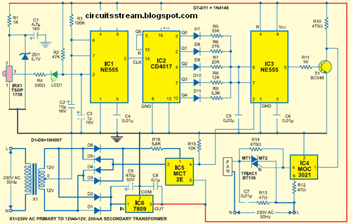
Remote-Controlled Fan Regulator Circuit Diagram. Using this circuit, you can change the speed of the fan from your couch or bed. Infrared receiver module TSOP1738 is used to receive the infrared signal transmitted by remote control. The circuit is powered by regulated 9V. The AC mains is stepped down by transformer X1 to deliver a secondary output of 12V-0-12V. The transformer output is rectified by full-wave rectifier comprising diodes D1 and D2, filtered by capacitor C9 and regulated by 7809 regulator to provide 9V regulated output. Any button on the remote can be used for controlling the speed of the fan. Pulses from the IR receiver module are applied as a trigger signal to timer NE555 (IC1) via LED1 and resistor R4.

Remote-Controlled Fan Regulator Circuit Diagram:

Regulator Circuit Diagram
 
IC1 is wired as a monostable multivibrator to delay the clock given to decade counter-cum-driver IC CD4017 (IC2).Out of the ten outputs of decade counter IC2 (Q0 through Q9), only five (Q0 through Q4) are used to control the fan. Q5 output is not used, while Q6 output is used to reset the counter. Another NE555 timer (IC3) is also wired as a monostable multivibrator. Combination of one of the resistors R5 through R9 and capacitor C5 controls the pulse width.  The output from IC CD4017 (IC2) is applied to resistors R5 through R9. If Q0 is high capacitor C5 is charged through resistor R5, if Q1 is high capacitor C5 is charged through resistor R6, and so on.

Optocoupler MCT2E (IC5) is wired as a zero-crossing detector that supplies trigger pulses to monostable multivibrator IC3 during zero crossing. Opto-isolator MOC3021 (IC4) drives triac BT136. Resistor R13 (47-ohm) and capacitor C7 (0.01µF) combination is used as snubber network for triac1 (BT136). As the width of the pulse decreases, firing angle of the triac increases and speed of the fan also increases. Thus the speed of the fan increases when we press any button on the remote control. Assemble the circuit on a general-purpose PCB and house it in a small case such that the infrared sensor can easily receive the signal from the remote transmitter.


read more...

1+1 Regulator Handles Two Input Voltages

Regulator Handles Two Input Voltages circuit in Fig 1 supplies both 3.3 and 5V to transitional circuits that employ both the new 3.3V and older 5V devices. Additionally, because the regulator accepts either 3.3 or 5V inputs, you could plug it into either a new 3.3V system or an old 5V system.The circuit consists of two sections: a dc/dc converter and a double-pole, double-throw (dpdt) switch. The dpdt switch comprises a pair of dual n-channel MOSFETs (Q2 and Q3) and their associated high-side drivers.

1+1 Regulator Handles Two Input Voltages Circuit Diagram:

Voltages Circuit Diagram

Upon power-up, the comparator in IC2 determines the state of the circuit. The comparator’s output, IC2 pin 6, goes to the input of the MOSFET driver, IC1. The driver internally generates a gatedrive voltage 8.8V above the device’s supply voltage. This high voltage drives the appropriate MOSFETs in Q2 and Q3.

IC2 is also the heart of a flying-capacitor, buck/boost dc/dc converter. Unlike other switching-regulator schemes, this topology needs no transformers. Transistor Q1 controls this section’s output voltage, VS. When VIN is at 5V, Q1 is off, forcing the section to operate as a step-down converter. In this mode, the section produces 3.3V, which goes to the output through Q3B. Also in this mode, 5V power goes directly through Q2A, and Q2B and Q3A are both off.

When VIN is 3.3V, IC1 turns on Q1, shorting out the 140-kΩ resistor and forcing the dc/dc-converter section into step-up mode. In this mode the converter section generates 5V at VS, powering the 5V output via Q2B. Also in this mode, 3.3V goes directly from the circuit’s input to the output via Q3A. Q2A and Q3B are both off.No-load quiescent current consumption is approximately 500 μA.

Lower-frequency converters would reduce power consumption at the expense of a larger inductor. The efficiency of the dc/dc-converter section is 73% in either mode. But because this power accounts for only half of the circuit’s output power, the circuit’s overall efficiency is approximately 80% with VIN=3.3V and 86% with VIN=5V.


read more...

Simple Electrification Unit Circuit Diagram:

The circuit is intended for carrying out harmless experiments with high-voltage pulses and functions in a similar way as an electrified fence generator. The p.r.f. (pulse repetition frequency) is determined by the time constant of network R1-C3 in the feedback loop of op amp IC1a: with values as specified, it is about 0.5 Hz. The stage following the op amp, IC1b, converts the rectangular signal into narrow pulses. Differentiating network R2-C4, in conjunction with the switching threshold of the Schmitt trigger inputs of IC1b, determines the pulse period, which here is about 1.5 ms. The output of IC1b is linked directly to the gate of thyristor THR1, so that this device is triggered by the pulses.

The requisite high voltage is generated with the aid of a small mains transformer, whose secondary winding is here used as the primary. This winding, in conjunction with C2, forms a resonant circuit. Capacitor C3 is charged to the supply voltage (12 V) via R3.When a pulse output by IC1b triggers the thyristor, the capacitor is discharged via the secondary winding. The energy stored in the capacitor is, however, not lost, but is stored in the magnetic field produced by the transformer when current flows through it. When the capacitor is discharged, the current ceases, whereupon the magnetic field collapses. This induces a counter e.m.f. in the transformer winding which opposes the voltage earlier applied to the transformer.

Simple Electrification Unit Circuit Diagram:


 Simple Electrification Unit Circuit Diagram
 
This means that the direction of the current remains the same. However, capacitor C2 is now charged in the opposite sense, so that the potential across it is negative. When the magnetic field of the transformer has returned the stored energy to the capacitor, the direction of the current reverses, and the negatively charged capacitor is discharged via D1 and the secondary winding of the transformer. As soon as the capacitor begins to be discharged, there is no current through the thyristor, which therefore switches off. When C2 is discharged further, diode D1 is reverse-biased, so that the current loop to the transformer is broken, whereupon the capacitor is charged to 12 V again via R3. At the next pulse from IC1b, this process repeats itself.

Since the transformer after each discharge of the capacitor at its primary induces not only a primary, but also a secondary voltage, each triggering of the thyristor causes two closely spaced voltage pulses of opposite polarity. These induced voltages at the secondary, that is, the 230 V, winding, of the transformer are, owing to the higher turns ratio, much higher than those at the primary side and may reach several hundred volts. However, since the energy stored in capacitor C2 is relatively small (the current drain is only about 2 mA), the output voltage cannot harm man or animal. It is sufficient, however, to cause a clearly discernible muscle convulsion.


read more...

Power-Back Surge Protection

Power-Back Surge Protector is a simple yet effective solution for protecting your valuable and sensitive electric/electronic systems. Power-Back Surge typically occurs when power returns after a power-cut (black out) and connected equipments receives a surge of electricity at an over-voltage level, which can be very damaging. Usually, power-back surges are created by the utility, when it restores supply at an above normal voltage level inorder to compensate for the demand as connected equipment restarts at the same time. The author took this little circuit personally to protect numerous lab equipments including his fave DSO!

Power-Back Surge Protection Circuit Diagram:

Power-Back Surge Protection Circuit Diagram
 
The circuit is designed to be constructed in a small module structure with an onboard electromagnetic relay as the primary switching device. The design is centered around (again) the famed 555 timer, wired as a bi-polar latch switch with its two comparator inputs tied together and biased at 1/2 Vcc through a resistive-potential divider. Since the threshold comparator will trip at 2/3 Vcc and the trigger comparator will trip at 1/3 Vcc, the bias provided by the resistors are centered within the comparators trip limits. The module does need a source of external power for operation, and so a “clean” 5v dc supply is preferred here as the power supply for the entire circuit.

Protection Circuit Diagram

However, note that the onboard miniature relay cannot drive grid-supply powered “goliath” loads without the help of an external heavy-duty switching relay. It is better to use a T90 type (5v dc) heavy-duty relay as the external relay, because the type can handle too much power efficiently.

Working of the circuit is very simple. Initially when the circuit is powered up or when power supply is resumed, the relay remains in the de-energized state. This prevents the power supply from reaching to the connected load. When the push-to-on switch (a good quality momentary push button switch required) is depressed, the circuit turns to active mode, relay is energized, and hence power supply is extended to the connected load. The red LED in the circuit is the “power in” status indicator, and the green LED is the “power out” status indicator.

Surge Protection Circuit Diagram

Author used an “O/E/N” pcb relay (part # 46-05-2CE) in the prototype, and a “Tyco” T90 pcb relay (part# T90N5D12-5) as the optional external relay. Photograph of the initial prototype with some components soldered at the bottom side of the perfboard (however, without the red indicator, push button switch, and headers) is shown below. Sorry have to be the potato picture as the finished system is in use now!

Author By: T.K. HAREENDRAN

read more...

Simple 3 Volts Car Adapter

This 3 volts Car Adapter circuit is based on a standard LT1074CT switching regulator IC. The schematic shows the LT1074CT used as a positive step-down or ‘buck’ converter. The ‘switcher’ is used to convert a +12-volt car battery voltage down to +3 volts for use with the personal hi-fi’s and handheld games for the author’s two boisterous children on long car journeys. Note at under ten years of age, children will rarely be hi-fi aficionado’s and are generally not concerned with any noise generated by the ‘switcher ‘circuit.

3 volts car adapter circuit diagram:


 3 volts car adapter circuit diagram

The circuit is connected to the car +12-V system via the cigarette lighter socket — is advisable to use a fused version of the cigarette lighter plug. The +12-V arrives on the board via screw- terminal block J2. Diode D2 provides a reverse voltage protection, while C3 decouples the input to the switcher IC.

The LT1074CT briskly switches the supply voltage on and off in response to the signal applied to its F/B input, to the extent that the average output voltage is at the required level. The values of potential divider resistors R1-R3 have been chosen to attenuate the output voltage so that there is 2.5 V at the F/B pin. The difference between the attenuated output voltage and the internal 2.5-V reference is used to control the modulation effect of the switcher.

Components R2 and C2 provide frequency stabilisation for the feedback loop. Inductor L1 along with the LT1074CT form the main switching components, while C1 provides decoupling for the output load. The 3-V output voltage is taken from screw terminal J1. With this circuit built, boxed up and installed in your car, you can look forward to possibly your first ‘quiet’ long car journey.


Author By: P. MARIAN
read more...

1.3 Volt Power Source

This is a replacement power source for 1.3V mercury cells or other small batteries. It has many uses and I use this circuit in my computer to power a front panel multi adapter which has a digital thermometer.

1.3 Volt Power Source Circuit Diagram:

Source Circuit Diagram
 
Notes
This circuit takes it power from a PC. The power connectors have colour coded wiring, red and black are the 5V supply, black and yellow are the 12V supply. These are extremely high current so absolute care must be taken to avoid short circuits and an inline fuse of 100mA is recommended.

The 1.3V is derived from a Red LED. When on and forward biased the LED's voltage drop between anode and cathode is about 1.9V, this is too high for mercury cell powered equipment, but fed in series with a 1N4148 signal diode drops around 0.6V, the supply is then ideal to drive battery powered peripherals.

This is not suitable for clocks, because when the computer is turned off the 5V supply is also switched off. It is however ideal for the independent temperature displays often included with PC preripherals such as case mounted usb connectors.

Connections
Please note that if you choose to solder connections onto the battery compartment like me it will void the warrantry of your equipment. Do so, only at your own risk. Below is a close up shot of the battery connections.

Power Circuit Diagram

Soldering here requires care, as excess heat will melt the surrounding plastic and you will be working in a small space, typically less than the width of a battery or less than 10mm. Flexible stranded wire is the best to use here. Below is the finished view of my front panel adapter.

1.3 Volt Power Source Circuit Diagram


Author By: Andy Collinson

read more...

Simple Portable Power Inverter

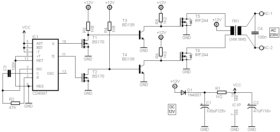
Recently, my neighbor expressed a deep interest in building a low-power inverter from scratch. This portable power inverter takes the dc output from a low-voltage accumulator and creates a stable 230-VAC/50-Hz mains suitable for powering small items of equipment. As several inverter designs have already been published on the web, the goal here was to make the design easily accessible to others by using familiar and easily sourced components available to novices and hobbyists everywhere. Here is the design that uses readily obtainable N-type FETS and an inexpensive CMOS chip to generate the square wave signals. Because the square wave signals are generated by a single chip, it can easily be modified for 50 Hz or 60 Hz, either 115 V or 230 V, and a broad range of input voltages. 

Portable Power Inverter Circuit Diagram:

Inverter Circuit Diagram

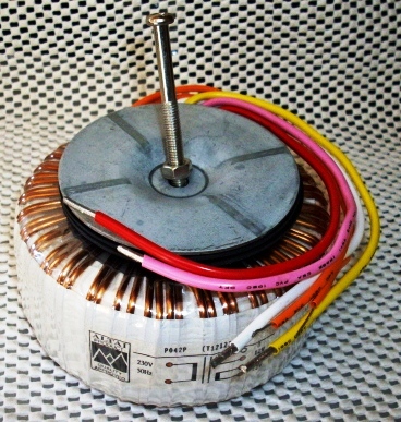
The circuit is built around the monostable/astable multivibrator CD4047 (IC1). The resistor (R2) and capacitor (C3), connected to pins 2 and 3, will decide the frequency of the astable output pulses (here, it is at about 50 Hz). IC1 gives two similar frequency outputs at pins 10 and 11 (phase of the Q and Q signals varies about 180 degrees). The square wave output signals are processed by the two-channel transistor banks (T1-T3-T5 and T2-T4-T6) to drive the power transformer (TR1). In my prototype, TR1 is a 60-VA toroidal transformer with a nominal 12-V rms secondary and 5-A current. I have powered up the inverter with an SMF battery of 12 V close to 7 Ah and successfully powered one 230-V/40-W lightbulb. The efficiency looks promising with neither the MOSFETs nor the transformer getting hotter than warm.


Power Inverter Circuit DiagramPortable Circuit Diagram

Parts List:
 
IC1: CD4047N
T1, T2: BS170
T3, T4: BD139 (or D400)
T5, T6: IRFZ44N
D1: 1N4007
C1: 100 uF/25 V
C2: 47 uF/16 V
C3: 100 nF/63 V
C4: 100 nF/400 V~
R1: 1K2
R2: 47K (change to 39K for 60 Hz)
R3, R4: 1K8
R5, R6: 1K2
TR1: (see text)

Power Circuit Diagram

Because the inverter has fatal mains voltages present, it is highly recommended that it be put into a metal enclosure (with adequate vent holes). The largest component is the toroidal transformer, which should be securely mounted to the chassis. A proper (TO-220) heatsink should be used with the FETs (T5-T6). Note that both the upper and lower FETs can be bolted into a single (TO220x2) heatsink plate, provided that they are insulated from each other and from the heatsink plate. The proposed portable power inverter is intended to be used when there is no option to use ac mains for certain low-wattage devices (for example, as an in-car/camping inverter). I am happy to receive feedback from readers in the hope that this primitive design will evolve into an efficient unit!

Author By: T.K. HAREENDRAN


read more...

12 Volts Voltage Regulator Car Adapter

A simple 12 volts voltage regulator car adapter circuit can be used to power your electronic devices from your car can be designed using few common electronic components.

12 Volts Voltage Regulator Car Adapter Circuit Diagram:

12 Volts Voltage Regulator Car Adapter Circuit Diagram

This 12 volts voltage regulator car adapter circuit use a 12.7 volts zener diode but maybe you can’t find a 12,7 volts zener , so in that case you can use a 12 v or 13 volts zener diode . If you will use a 12 volts zener you will need to stick in another diode like 1N4001 (in this case the output voltage will be a little under 12 ) and if you will use a 13 volts zener the output voltage will be around 12.3 volts.
read more...

Dropout Adjustable Breadboard Power Supply

This project details the design of a very low dropout adjustable power supply. A good power supply is essential to electronic projects. While there are many existing designs for adjustable power supplies, this one makes improvements that make it more useful for hobby designs.

Power Supply

MIC2941 regulator has guaranteed 1.25A output
Low dropout, only 40mV - 400mV compared to 1.25V - 2.0V for LM317. This means you can use a wider range of output voltages including generating 3.3V from as low as 3.7V (such as 3 AA's or a lithium ion battery)!

Breadboard Power Supply


Short circuit and overheating protection
Input diode to protect circuitry from negative voltages or AC power supplies.
2.1mm DC jack and terminal connector for voltage inputs
Two indicator LEDs for high and low voltages
Output selection switch to select from 3.3v, 5v and Adjustable
On-board potentiometer for adjusting voltage from 1.25V up to within 0.5V of the input voltage. (20V max) On/Off switch for entire board.

read more...

LM338 Power Supply +13.8V 5A

This ac to dc power supply can output 5A in continous operation and 12A peak current. This kind of dc power supplies uses a PCB so you can use two case types for IC1, TO-220 or TO-3. The regulation of this 12 volt power supply is made with TR1 ( multiturn ). IC1 must be placed on proper heatsink.

LM338 Power Supply Circuit Diagram :

LM338

read more...

Adjustable Symmetrical Power Supply Using LM317 and LM337

The circuit was designed to provide an adjustment with a power supply that is symmetrically designed while providing a voltage range of 1.25V to 30V at 1A current. LM317 – an adjustable 3-terminal positive voltage regulator capable of supplying in excess of 1.5A over an output voltage range of 1.2V to 37V and requires only two external resistors to set the output voltage due to its internal current limiting, thermal shutdown and safe area compensation, making it essentially blow-out proof LM337 – an adjustable 3-terminal positive voltage regulator capable of supplying in excess of 5A used as battery chargers, constant current regulators, and adjustable power supplies due to its features such as protected output from short circuit, product enhancement tested, current limit constant with temperature, guaranteed thermal regulation, adjustable output down to 1.2V, guaranteed 5A, and guaranteed 7A peak output current.

Adjustable Symmetrical Power Supply Using LM317 and LM337:

LM317 and LM337

The circuit will serve as a voltage converter with an input voltage of 35 V to produce an output voltage of 1.25 V to 30 V. The positive voltage is being handled by LM317 IC while the negative voltage is handled by LM337. The circuit can provide an output current of 1 A. During the production of 1 A current, the regulator is dissipating too much heat and without the presence of a heatsink, the regulator may get damaged.

Using these types of regulators provide features such as low noise and low price in the market. It can be made operational even with few components used. The only disadvantage that it will impose is the poor conversion efficiency. With the output of 35 V to 5 V, the efficient ratio of the output power with the input power is less than 42%. This is the reason why the switching regulator became cheap recently although the number of external components to be connected is minimally increased. These regulators will work with better efficiency when used in case where current is more than 1A for more than 15 V and 0.4 A for less than 15 V from the power supply. Each regulator is adjusted for single positive and negative voltage output using the 10K ohms potentiometers RV1 & RV2. For dual outputs, a dual connected potentiometer RV3 is made to operate by switch S1. The visual indication on the voltmeter V1 is shown using the switch S2.

R1-2=270ohms
R3-4=2.2Kohms
R5-6=10Kohms
C1-5=100uF/63V
C2-4=100nF/100V
C3-8=10uF/25V
C6-10=100uF/63V
C7-9=100nF/100V
RV1-2=10Kohms Lin.
RV3=2X10Kohms Lin.
IC 1=LM 317T
IC 2=LM 337T
D1-2=1N4001
D3-4=1N4001
L1-2=LED 3mm
F1-2=1A slow Blow Fuse
S1-2=2X ON-ON SW
V1=0-30V DC Voltmeter

The adjustable symmetrical power supply is suitable to be used in audio amplifiers, microphone amplifiers, op-amp applications, impedance converters and other devices that require regulated positive and negative DC supply, since the output current is 1 A.


read more...

Build A UPS Power Supply

This circuit is a simple form of the commercial UPS, the circuit provides a constant regulated 5 Volt output and an unregulated 12 Volt supply. In the event of electrical supply line failure the battery takes over, with no spikes on the regulated supply.

UPS

This circuit can be adapted for other regulated and unregulated voltages by using different regulators and batteries. For a 15 Volt regulated supply use two 12 Volt batteries in series and a 7815 regulator. There is a lot of flexibility in this circuit.

TR1 has a primary matched to the local electrical supply which is 240 Volts in the UK. The secondary winding should be rated at least 12 Volts at 2 amp, but can be higher, for example 15 Volts. FS1 is a slow blow type and protects against short circuits on the output, or indeed a faulty cell in a rechargeable battery. LED 1 will light ONLY when the electricity supply is present, with a power failure the LED will go out and output voltage is maintained by the battery. The circuit below simulates a working circuit with mains power applied:
Power Supply

Between terminals VP1 and VP3 the nominal unregulated supply is available and a 5 Volt regulated supply between VP1 and VP2. Resistor R1 and D1 are the charging path for battery B1. D1 and D3 prevent LED1 being illuminated under power fail conditions. The battery is designed to be trickle charged, charging current defined as :-

(VP5 - 0.6 ) / R1
where VP5 is the unregulated DC power supply voltage.

D2 must be included in the circuit, without D2 the battery would charge from the full supply voltage without current limit, which would cause damage and overheating of some rechargeable batteries. An electrical power outage is simulated below:

Circuit Diagram for UPS

Note that in all cases the 5 Volt regulated supply is maintained constantly, whilst the unregulated supply will vary a few volts.

Standby Capacity
The ability to maintain the regulated supply with no electrical supply depends on the load taken from the UPS and also the Ampere hour capacity of the battery. If you were using a 7A/h 12 Volt battery and load from the 5 Volt regulator was 0.5 Amp (and no load from the unregulated supply) then the regulated supply would be maintained for around 14 hours. Greater A/h capacity batteries would provide a longer standby time, and vice versa.
read more...

Power Supply with High Voltage Isolation

Occasionally you come across some unusual  situations when setting up measurement  systems. The author once had to set up a system to register the vibrations and strain supposed to be  present in a contactor that operated at a voltage of 25 kVAC.

Power Supply with High Voltage Isolation Circuit Diagram: 

Power Supply Circuit Diagram

One of the biggest problems with this project turned out to be the power supply for  the measurement system. Since it required  a power of about 30 W it wasn’t possible to  use batteries since the system had to operate  for many hours at a time. A logical solution  would seem to be to use an isolating trans-former, but still.25 kVAC means a peak volt-age approaching 40 kV, and on top of that  you would have to include a safety margin. In  addition, everything that is connected to high  voltage lines should also be able to withstand  lighting strikes!

Consequently the isolation should be able to  cope with a test voltage of 150 kV, which is a  lot to ask of the isolating material.

After extensive research no supplier could be  found for a transformer rated at 50 W, 230 V  primary, 12 V secondary and an isolation of  25 kVAC. Because of this, a dynamic system  had to be used that unfortunately suffers a  bit from wear and tear. This system consists  of a 50 W 3-phase motor connected up via an  isolating drive-shaft to a 30 W generator (a  3-phase servo motor that was used as a generator), which provides the power for the data  logger and associated electronics.

Because a 3-phase generator was used, the  voltage obtained after full-wave rectification (via D1 and D4 to D8) already looked good,  also because the revs of the generator was  fairly high. The secondary supply can there-fore remain fairly simple. The main supply of 9 VDC is stabilised by IC3, an LM317T. From  there it is fed to a few small DC/DC modules  (IC1, IC4, IC5), which supply voltages of +5 V,  +30 V and -9 V, which are required by the other parts of the circuit. IC2 (LM566, a volt-age controlled oscillator) makes LED D2 flash  when the supply voltage is present.

read more...

Switching Power Supply Using MC33374

This switching power supply circuit diagram is based on the MC33374 high power voltage switching regulator IC manufactured by Motorola Semiconductor. This MC33374 switching power supply circuit will provide a maximum output power around  90 W and require few external components .

The MC33374 switching regulator IC is a monolithic high voltage power switching regulators that combine the required converter functions with a unique programmable state controller .

The MC33374 switching regulator IC is designed to operate directly from a rectified AC line source, and in flyback converter applications are capable of providing an output power in excess of 150 W with a fixed AC input of 100 V, 115 V, or 230 V, and in excess of 90 W with a variable AC input that ranges from 85 V to 265 V.

Circuit Diagram: 

MC33374

Parts

MC33374

The MC33374 switching regulator offers features like  : Programmable State Controller , On–Chip 700 V SENSEFET Power Switch Circuit , Rectified AC Line Source Operation from 85 V to 265 V , On–Chip 700 V Active Off–Line Start–Up Circuit , Latching PWM for Double Pulse Suppression , Cycle–By–Cycle Current Limiting , Input Undervoltage Lockout with Hysteresis, Non–Latching Internal Thermal Shutdown .

This MC33374 switching power supply circuit has a efficiency of 83.2 % at 115 V AC input voltage and a 85.4 % efficiency at 230 V with  IO= 6 A.

The output voltage of this switching power supply is 15 volts and the maximum output current is 6 A .

The hard part of these switching power supply circuit is   to design the T1 transformer  , but you have the design data for that bellow , or you can buy a transformer from Coilcraft.

Z1 is a zenner diode and is used to limit the voltage on Pin 5 and a damper circuit consisting of resistor R2 and capacitor C2.


read more...

3 to 12 Volts Converter with LM2700

This is very simple electronic circuit diagram for 3 to 12 volts converter, this circuit simple and high efficiency step-up dc dc converter circuit that require few external components can be designed using the LM2700 step-up DC/DC converter with a 3.6A, 80mohms internal switch and pin selectable operating frequency.

3 to 12 Volts Converter Circuit Diagram:

LM2700
 
With the ability to produce 500mA at 8V from a single Lithium Ion battery, the LM2700 is an ideal part for biasing LCD displays. The LM2700 can be operated at switching frequencies of 600kHz and 1.25MHz allowing for easy filtering and low noise. An external compensation pin gives the user flexibility in setting frequency compensation, which makes possible the use of small, low ESR ceramic capacitors at the output.

This circuit can be used for handheld devices and some other portable applications. This step-up DC DC converter will provide a 12 volts DC output voltage from an input voltage range between 2.5 to 4.2volts.
read more...

230 V AC To 400 V DC Power Supply

 230 V AC To 400 V DC Power Supply Circuit Diagram:
 
Power Supply Circuit Diagram

Description:
A lot of students are who don't know how to convert 230 volt AC to 400 DC. So today i am published  ' 230 V AC to 400 V DC circuit diagram ' on my blog. Working principle of this circuit diagram is very simple. You already knew the working principle of a bridge rectifier. This circuit is same as bridge rectifier and the working principle is also same. The fuse is used to protect the circuit, if the current is greater than 1 A.

Parts List

Component No:Value
F11 A
B1IN4007 
C1470MF/450V 
V1230 V AC 
read more...
 
Copyright © 2019 W3circuits.blogspot.com • All Rights Reserved.
back to top