Showing posts with label Computer Related. Show all posts

1.3 Volt Power Source

This is a replacement power source for 1.3V mercury cells or other small batteries. It has many uses and I use this circuit in my computer to power a front panel multi adapter which has a digital thermometer.

1.3 Volt Power Source Circuit Diagram:

Source Circuit Diagram
 
Notes
This circuit takes it power from a PC. The power connectors have colour coded wiring, red and black are the 5V supply, black and yellow are the 12V supply. These are extremely high current so absolute care must be taken to avoid short circuits and an inline fuse of 100mA is recommended.

The 1.3V is derived from a Red LED. When on and forward biased the LED's voltage drop between anode and cathode is about 1.9V, this is too high for mercury cell powered equipment, but fed in series with a 1N4148 signal diode drops around 0.6V, the supply is then ideal to drive battery powered peripherals.

This is not suitable for clocks, because when the computer is turned off the 5V supply is also switched off. It is however ideal for the independent temperature displays often included with PC preripherals such as case mounted usb connectors.

Connections
Please note that if you choose to solder connections onto the battery compartment like me it will void the warrantry of your equipment. Do so, only at your own risk. Below is a close up shot of the battery connections.

Power Circuit Diagram

Soldering here requires care, as excess heat will melt the surrounding plastic and you will be working in a small space, typically less than the width of a battery or less than 10mm. Flexible stranded wire is the best to use here. Below is the finished view of my front panel adapter.

1.3 Volt Power Source Circuit Diagram


Author By: Andy Collinson

read more...

Computer Room Temperature Control Using TC620

Here is a very simple electronic circuit project for Computer room temperature control circuit using TC620 temperature sensor.

Computer Room Temperature Control Using TC620:

Computer

As shown in the figure, the circuit consists of the temperature sensor, control devices, the upper and lower temperature display, relay control motor circuit, waves analog voice circuit and AC buck rectifier circuit.
read more...

Simple But Digital Electronic Lock

This Electronic Circuit Project of simple but digital electronic Lock circuit. The digital lock shown below uses 4 common logic ICs to allow controlling a relay by entering a 4 digit number on a keypad. The first 4 outputs from the CD4017 decade counter (pins 3,2,4,7) are gated together with 4 digits from a keypad so that as the keys are depressed in the correct order, the counter will advance.

 As each correct key is pressed, a low level appears at the output of the dual NAND gate producing a high level at the output of the 8 input NAND at pin 13. The momentary high level from pin 13 activates a one shot circuit which applies an approximate 80 millisecond positive going pulse to the clock line (pin 14) of the decade counter which advances it one count on the rising edge.

A second monostable, one shot circuit is used to generate an approximate 40 millisecond positive going pulse which is applied to the common point of the keypad so that the appropriate NAND gate will see two logic high levels when the correct key is pressed (one from the counter and the other from the key).

Digital Electronic Lock Circuit Diagram:

Electronic Circuit Diagram:


The inverted clock pulse (negative going) at pin 12 of the 74C14 and the positive going keypad pulse at pin 6 are gated together using two diodes as an AND gate (shown in lower right corner). The output at the junction of the diodes will be positive in the event a wrong key is pressed and will reset the counter. When a correct key is pressed, outputs will be present from both monostable circuits (clock and keypad) causing the reset line to remain low and allowing the counter to advance.

However, since the keypad pulse begins slightly before the clock, a 0.1uF capacitor is connected to the reset line to delay the reset until the inverted clock arrives. The values are not critical and various other timing schemes could be used but the clock signal should be slightly longer than the keypad pulse so that the clock signal can mask out the keypad and avoid resetting the counter in the event the clock pulse ends before the keypad pulse. The fifth output of the counter is on pin 10, so that after four correct key entries have been made, pin 10 will move to a high level and can be used to activate a relay, illuminate an LED, ect.

At this point, the lock can be reset simply by pressing any key. The circuit can be extended with additional gates (one more CD4011) to accept up to a 8 digit code. The 4017 counting order is 3 2 4 7 10 1 5 6 9 11 so that the first 8 outputs are connected to the NAND gates and pin 9 would be used to drive the relay or light. The 4 additional NAND gate outputs would connect to the 4 remaining inputs of the CD4068 (pins 9,10,11,12). The circuit will operate from 3 to 12 volts on 4000 series CMOS but only 6 volts or less if 74HC parts are used. The circuit draws very little current (about 165 microamps) so it could be powered for several months on 4 AA batteries assuming only intermittent use of the relay.


read more...

Reset Protection For Computers

It is very simple and low-cost Electronic circuit diagram for Reset Protection For Computers. This protection circuit is inserted between the reset switch and the motherboard. The earth connection of the computer must be linked to terminal of the protection circuit. The protection circuit can draw its power from the computer supply. When the circuit has been fitted, operation of the reset switch will not immediately restart the computer. Instead, a buzzer will sound to alert you to the reset operation.

Reset Protection For Computers Circuit Diagram:

Computers Circuit Diagram

The buzzer is actuated for 4 s by monostable IC1A, which is triggered by the reset switch. During these 4 s, the output, pin 5, of IC1A ensures that the reset function, pin 10, of IC1B is disabled. When the reset switch is operated again, monostable IC IB will be triggered and this starts the reset procedure.

Transistor T2 is then switched on for 0.5 s and the buzzer is deactuated via Rll and D4. The circuit around T1 and N4 ensures that IC1A can accept trigger pulses again 10 s after the mono time of IC1B has lapsed. This arrangement prevents, for example, children operating the reset switch.


read more...

How to Build a UPS for USB devices

Portable systems often include circuitry that derives power from an external source, such as USB. When the system disconnects from the USB supply, a battery takes over and supplies current via a dc/dc converter. A diode-OR connection (Figure 1 offers the easiest way to ensure that the supply voltage doesn't sag during this switchover to the battery. The diode's forward voltage drop, however, can reduce battery life and efficiency.
 
Build a UPS for USB devices

A diode-OR connection is effective but lossy.


Computer Related
 A boost-converter circuit is an improvement over the simple diode-OR connection.

The single-cell, boost-converter circuit with external PFET (Figure 2) is an improvement over the diode-OR connection. The PFET, Q1, coupled with IC1's internal gain block, forms a linear regulator. The USB power supply has a diode-OR connection to Q1's source. Setting the boost converter's output to 3.4V allows the drain of Q1 to regulate to 3.3V. This configuration produces negligible loss in Q1. The bus-supply voltage available to USB devices ranges from 4.4 to 5.25V.

When you connect the bus, it forward-biases D1 and causes the boost converter to idle. The converter continues to idle as long as its output remains above the 3.4V regulation point. The bus supply serves the load and activates the current source to charge the battery.

Computer Related
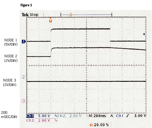
These waveforms (bottom trace, load voltage) show that the load current suffers no interruption during a switchover from USB to battery.

Adjusting R1 allows you to set the current-source output to charge the nickel-metal-hydride cells at a level one-tenth the battery's capacity. Disconnecting the circuit from the USB supply causes the boost converter to cease idling and supply current to the load via the battery. Figure 3 shows that the load current suffers no interruption during a switchover from USB to battery.


read more...

Digital But Simple Electronic Lock

The digital lock shown below uses 4 common logic ICs to allow controlling a relay by entering a 4 digit number on a keypad. The first 4 outputs from the CD4017 decade counter (pins 3,2,4,7) are gated together with 4 digits from a keypad so that as the keys are depressed in the correct order, the counter will advance.

As each correct key is pressed, a low level appears at the output of the dual NAND gate producing a high level at the output of the 8 input NAND at pin 13. The momentary high level from pin 13 activates a one shot circuit which applies an approximate 80 millisecond positive going pulse to the clock line (pin 14) of the decade counter which advances it one count on the rising edge.

Digital But Simple Electronic Lock Circuit Diagram

Electronic Lock Circuit Diagram


A second monostable, one shot circuit is used to generate an approximate 40 millisecond positive going pulse which is applied to the common point of the keypad so that the appropriate NAND gate will see two logic high levels when the correct key is pressed (one from the counter and the other from the key). The inverted clock pulse (negative going) at pin 12 of the 74C14 and the positive going keypad pulse at pin 6 are gated together using two diodes as an AND gate (shown in lower right corner). The output at the junction of the diodes will be positive in the event a wrong key is pressed and will reset the counter.

When a correct key is pressed, outputs will be present from both monostable circuits (clock and keypad) causing the reset line to remain low and allowing the counter to advance. However, since the keypad pulse begins slightly before the clock, a 0.1uF capacitor is connected to the reset line to delay the reset until the inverted clock arrives. The values are not critical and various other timing schemes could be used but the clock signal should be slightly longer than the keypad pulse so that the clock signal can mask out the keypad and avoid resetting the counter in the event the clock pulse ends before the keypad pulse.

The fifth output of the counter is on pin 10, so that after four correct key entries have been made, pin 10 will move to a high level and can be used to activate a relay, illuminate an LED, ect. At this point, the lock can be reset simply by pressing any key.

The circuit can be extended with additional gates (one more CD4011) to accept up to a 8 digit code. The 4017 counting order is 3 2 4 7 10 1 5 6 9 11 so that the first 8 outputs are connected to the NAND gates and pin 9 would be used to drive the relay or light. The 4 additional NAND gate outputs would connect to the 4 remaining inputs of the CD4068 (pins 9,10,11,12). The circuit will operate from 3 to 12 volts on 4000 series CMOS but only 6 volts or less if 74HC parts are used. The circuit draws very little current (about 165 microamps) so it could be powered for several months on 4 AA batteries assuming only intermittent use of the relay.


read more...
 
Copyright © 2019 W3circuits.blogspot.com • All Rights Reserved.
back to top