Showing posts with label Video. Show all posts

VGA Monitor Splitter and Extender

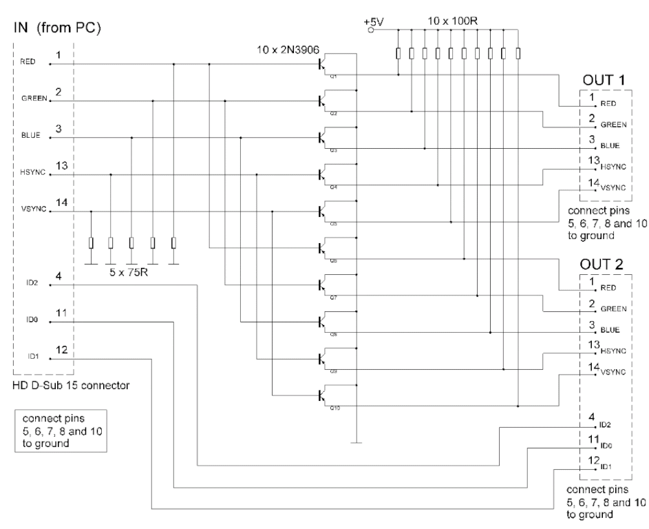
The circuit was designed to provide distribution, extension and splitting of personal computer video output to two or more monitors.
  • Super Video Graphics Array (SVGA) – defined in 1989 as a set of graphic standards that supports 800 X 400 resolution or 480,000 pixels with support for 256 colors or a palette of 16 million colors.
  • Pixel – short for picture element, is the smallest point or single item of information in a graphic image and the basic unit of programmable color on a computer image or computer display.
  • 2N3906 – a common PNP BJT transistor intended for medium voltage, lower current and power, which can operate at moderately high speeds, used for general purpose switching and low-power amplifying applications.
The circuit may also be called as video port expander, multiple monitor, PC video splitter, LCD Y splitter, etc. It provides the same high resolution image to several monitors using a single PC. Each line of the SVGA card of the analog output stage of PC contains 75 ohm impedance being obtained from the signal sources.

The transistors will not contribute as additional loads as they are having very high input impedances. The parameters being shared are the primary colors which consist of Red, Green and Blue, the horizontal synchronization and the vertical synchronization. Since the three ID connections are supposed to be connected to less advance and cheaper monitors, they can be excluded in the circuit.

VGA Monitor Splitter and Extender Circuit Diagram:

VGA Circuit Diagram
 
The PNP switching transistor 2N3906 forms the emitter-follower mode of ten transistors. They are utilized due to their low current having a maximum of 200 mA, low voltage with a maximum of 40 Volts, low cost, versatile and efficient, although they are not the best possible choice. It is preferable to use faster transistors when dealing with higher pixel rates because high input resistances will be supplied by higher gain.

The resolution entirely dictates the quality of a display system as to how many bits are used to represent each pixel and how many pixels it can display. To prevent RF interference on the circuit, as the monitor operates in radio frequency, a metal casing should enclose the splitter circuit and eventually be connected to ground.

The circuit will require a power supply of 5 Volts and a current around 600 mA. The DC components in the output signals will not be considered as drawbacks since the splitter is working well with 1024×768 15” and 800×600 monitors. The 2N3906 transistor is intended for amplifier functions and high-speed switching in industrial applications. Since there are many standards that have followed, all are employing the standards of SVGA since 1990 which includes the eXtended Graphics Array (XGA) of IBM, Super XGA (SXGA), SXGA+, Ultra XGA (UXGA) and Quad XGA (QXGA).

This video splitter will be suitable for tradeshows, in-store displays or classrooms where high quality video on multiple monitors is need; for support with LCD flat panel monitors and DDC2B protocol; in digital signage applications with perfect resolution; for supporting 1900×1200 resolution without degradation; for burn-in of monitors after repair; and for support of stereo audio as well. 


read more...

Simple TV Muter

Many households are still graced by tube-type television sets. If you want to connect one of these large tellies to your stereo system to improve the sound quality, this is usually not a problem because there are plenty of SCART to Cinch adapters available in accessory shops. However, with some sets your pleasure is spoiled by the fact that the audio outputs of the SCART connector are not muted during channel switching. This can sometimes lead to nasty signal spikes, which can cause the loudspeakers of your stereo system to emit irritating popping and cracking noises. In such cases it is a good idea to fit your system with a mute circuit.

Fortunately, the right time to activate the mute circuit is defined by the fact that the happy zapper presses buttons on the remote control to switch channels, and the remote control emits IR signals. There are even inexpensive ready-made IR receiver modules available, such as the TSOP1136 used here, which produce trains of active-low pulses in response to such signals. About the circuit: when no IR signal is present, a capacitor is charged via P2 and a diode. IC1 is a comparator that compares this IR voltage (applied to its non-inverting input on pin 3) to a voltage applied to its other input on pin 2.

TV Muter Circuit diagram :

TV Muter Circuit diagram

This reference voltage, which can be adjusted with P1, determines the switching threshold of the comparator. If IC2 receives an IR signal, T2 conducts, and as a result the voltage on C1 drops rapidly below the threshold level set by P1. This causes T1 to change from its previous ‘on’ state to the ‘off’ state. As a result, the relay drops out and the audio link to the stereo system is interrupted for the duration of the noise interval. It’s all quite simple, as you can see. If you do not have a stabilized 5-V supply voltage available, you can use the circuit at the of the schematic diagram (with a 5-V voltage regulator) together with a simple (unstabilised) AC mains adapter that supplies a voltage in the range of 9 V to 12 V to the 7805 (IC3).

You can also use a relay with normally-closed contacts instead of normally-open contacts. In this case, simply swap the signals on pins 2 and 3 of IC1 so the relay pulls in when an IR signal is received instead of dropping out. This saves a bit of power because the relay is only energized during zapping. If you can’t find any worthwhile use for the second comparator of IC1, it’s a good idea to connect pin 6 to +5 V and pin 5 to ground. To improve noise immunity, you should shield the IR sensor so it is not exposed directly to light from a fluorescent fixture. link


read more...

Video Amplifier Using NJM41045

Here is a very simple Electronic Circuit Project of Video Amplifier based on the wideband 3-channel video amplifier IC manufactured by New Japan Radio Co. Ltd.

Video Amplifier Using NJM41045 Circuit Diagram:

Video-Amplifier
 
The NJM41045 video amplifier is suitable for the HD video application because of -3dB large-signal bandwidth of 400MHz.

The circuit can be powered entire from a single or dual power supply circuit , supporting an input voltage range between 4.5 to 9.5 for single power source and from +/-3 to +/-5 volts for dual power source .
 
read more...

Build Electronic Project for Home Made Movie Maker

Like real movies, this circuit makes use of a characteristic of the human eye and brain known as the persistence of vision. A sequence of still pictures is projected onto a screen in rapid succession. The pictures differ slightly from one another and the brain interprets the succession of still pictures as continuous motion.
Here the pictures are shadows cast by low-voltage lamps. There are four Lamps in all, which glow in sequence cyclically. This gives the illusion of a simple but realistic movie.

Fig. 1 shows the circuit for the movie maker. It is driven by clock pulses provided by NAND gates N1 and N2. The flickering frequency is adjustable through preset VR1. A suitable rate for perceiving continuous motion is 16 Hz. The clock pulses are fed to counter IC CD4022 (IC2). IC2 has eight outputs, but only the first four (0-3) are used in this circuit. The outputs go high one at a time, in sequence. The fifth output (output 4) is connected to the reset input so that the counter is immediately reset at the fifth count and the first output (output 0) goes high.

The counter outputs are fed to CD4049 hex buffer (IC3). The buffer outputs drive transistors T1 through T4 in a sequence. As each transistor conducts, the lamp connected to it glows. The lamps are rated at 0.3A so these provide enough light to operate the movie show in a dimly-lit room.

Fig. 1: Circuit for movie maker:

Circuit for movie maker

Assemble the circuit on a general-purpose PCB. Power-on the circuitusing switch S1 and make sure that the outputs of IC2 (0 through 3) are normally low but briefly go high three-four times within a second. Also ensure that the lamps flash one at a time in a repeating sequence. If the sequence appears to be wrong or any of the lamps fails to glow, check the wiring. The light shield and film holder can be made of a thin card, sheet metal or plywood. Strictly adhere to the various dimensions as shown in Fig. 2. Otherwise, the shadow images may fail to register properly when projected.

Use a plastic cabinet as shown in Fig. 3 to hold the circuit board and battery. Owing to the power requirements of the lamps, it is more economical to use four 1.5V cells in a battery box. Else, you can use a 6V power adaptor.

Fig. 2: Assembly arrangement:

Circuit-Assembly


There are two ways of mounting the lamps. The more satisfactory but more expensive method is to bolt the four lamps. Alternatively, drill four 1cm dia. holes on the front of the cabinet, wedge the base of the lamps in these holes and solder wire to the bases.

Fig. 3: Plastic case with assembled circuit:

assembled circuit

The easiest way to prepare the film frames is to photocopy the desired drawings onto transparent films. Alternatively, trace them on a transparent acetate film or draughtsman's film, using a fine marker pen. Align all the drawings on the frames and project onto the screen.

Fig. 3: Flim making:
Cirucit-making

Working of the circuit is simple. First of all, fix the clock frequency at about 16 Hz. Place the film on the holder. Ensure a distance of 12 cm between the screen and the assembled unit and power-on the circuit using switch S1. Now you can see your drawings as a short movie clip on the screen.

EFY note. We have tested this circuit without the mechanical arrangement.

 Source: EFY


read more...

Electronic Project of Picture Fixer Inverter

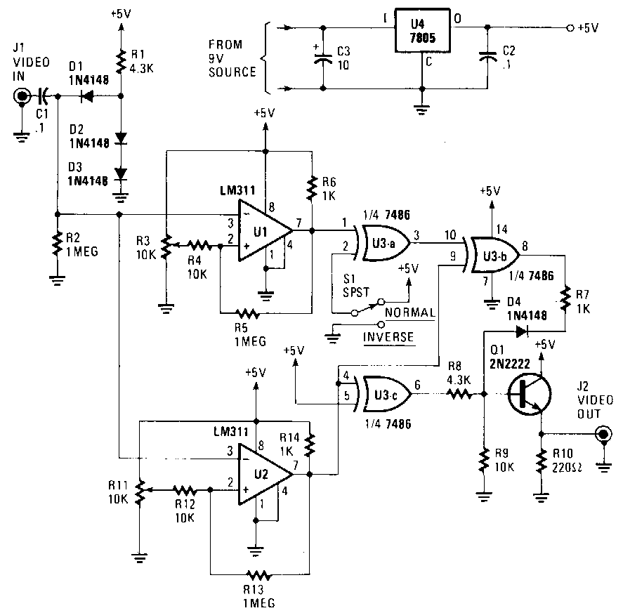
It is a simple and low-cost Electronic Circuit Project of Picture Fixer Inverter Circuit. The circuit will accept a video signal, separate the sync pulses, invert the video, and add new video to the old sync pulses. The video signal is brought in through Jl and applied to a clamping circuit consisting of Cl, Dl, D2,D3, Rl, and R2. The clamp circuit forces all of the sync pulses to align with the same de voltage level. With the video voltage clamped, the trip points of the comparators that follow can be set with trimmer resistors R3 and Rll.

Picture Fixer Inverter Circuit Diagram:

Picture Fixer Inverter Circuit Diagram

The resistors will not have to be readjusted. One comparator, Ul, is adjusted to change states with a change in either video or sync-pulse levels. The other comparator, U2, is adjusted to trip on changes of sync-pulse levels only. The output of Ul now consists of a logic level, 0 to +5 V, signal that contains both sync pulses and video. The composite signal is coupled to an EXCLUSIVE-OR gate, U3a, where it is either inverted or not inverted, depending upon the position of switch NORM/REV Sl.

The output, at pin 3 of U3a, is next sent to U3b. There the composite signal is combined with the sync-pulse only signal from U2. The EXCLUSIVE-OR action of U3b cancels out the sync pulses, leaving only video at the IC`s output. Since the sync pulses are inverted as they pass through U2, they must be inverted once more before being combined with the video signal.

That final inversion is performed bY U3c, and that device`s output is combined with that of U3b via D4, R7, RS, and R9. The newly combined signal is buffered bY emitter follower Ql, and sentto the outside world via ]2. The circuit can be powered by a 9-to 12-V wall-mount power supply. The supply voltage is regulated down to 5 V bY U4.


read more...

Video Tracer For Trouble-Shooting

This circuit was designed as an aid to installers and maintainers of video systems. It is basically a video sync separator (IC1) followed by a LED and buzzer driver (IC2, Q1 & Q2). In use, the device is connected to a video cable and if there is video present, the LED will flash at about 10Hz. If there is no video, the LED flashes briefly every couple of seconds. A buzzer can also be switched in to provide an audible indication. The buzzer is particularly useful when tracing cabling faults or trying to find a correct cable amongst many, where it is difficult to keep an eye on the LED.

Video Tracer Circuit Diagram
 

Video Tracer Circuit Diagram

Another use for the buzzer option is to provide a video fault indication. For example, it could be inserted in bridging mode, with switch S1 in high impedance mode (position 2) across a video line and set to alarm when there is no video present. If someone pulls out a cable or the video source is powered off, the alarm would sound. IC1 is a standard LM1881 video sync separator circuit and 75Ω termination can be switched in or out with switch S1a. The other pole of the switch, S1b, turns on the power. The composite sync output at pin 1 is low with no video input and it pulses high when composite sync is detected.

These pulses charge a 100nF capacitor via diode D1. When there is no video at the input, oscillator IC2b is enabled and provides a short pulse every couple of seconds to flash the LED. The duty cycle is altered by including D2, so that the discharge time for the 10μF capacitor is much shorter than the charge time. The short LED pulse is used as a power-on indicator drawing minimal average current. When video is present at the input, IC2b is disabled and IC2d is enabled. The output of IC2d provides a 10Hz square wave signal to flash the LED. The buzzer is controlled by switch S2. In position 2 the buzzer will sound when there is video at the input and in position 1 the buzzer will sound when there is no video at the input.


read more...

Simple Project to Build A Video Signal Emphasis

With this circuit we can amplification selectively the high signal of picture frequencies [Video] with result bigger clarity than this. The circuit should be placed between a Video unit and the reception Scart or the plug Video input of television receiver. The designing is simple, it’s based in three only transistor.

Video Signal Emphasis Circuit Diagram

Video Signal Emphasis Circuit Daigram

The first stage of Q1 function as isolator - adapter of input impedance. The second stage round the Q2 in common base connection which the gain is determined by the TR2. The TR1, R6 and C3 determine the frequency response. The third stage round the Q3 works as output buffer and 75-ohm line driver. The TR2 should be regulated in a place where the circuit output voltage, to be 1Vp-p, in 75 ohm load. The circuit functions with 12Volts - 50mA well stabilized.

Part List

R1=82ohm
R2=5.6Kohm
R3-9-11=2.7Kohm
R4=330ohm
R5=220ohm
R6=470ohm
R7=270ohm
R8=12Kohm
 R10=2.2Kohm
R12=180ohm
R13=68ohm
C1-4-5=100uF 16V
C2=2200uF 16V
C3=470pF ceramic
C6=470uF 16V
C7=220uF 16V
C8=100nF 100V MKT
TR1=250ohm trimmer
TR2=500ohm trimmer
D1=1N4148
Q1-2-3=BC547
J1-2=Female RCA jack
J3=2pin connector 2.54mm step

Video Signal Emphasis PCB 


Video Signal Emphasis PCB


read more...

Domestic TV Transmitter

This device connects to your audio input and output video from a cassette player or a camcorder and thus pass through the air to one or more televisions in the area of ​​a house. It is also useful to output the image and the sound of a computer to do multimedia presentations in several TV screens distributed in an enclosure. If you have a satellite TV service or premium cable system and want to watch programming on multiple televisions with a single tuner and / or decoder output can connect it to this project and enjoy the images in the house. Also useful in closed systems for security video, avoiding large number of cable runs.

Domestic TV Transmitter Circuit Diagram

TV Transmitter Circuit Daigram

As shown in the circuit diagram the circuit has several stages (a local oscillator, an FM modulator for audio an AM modulator for video, a mixer and an output amplifier) very simple to assemble. It has the controls necessary for achieving optimal fit and proper signal transmission.

Circuit Description:

The video signal entering through connector J1 is finished, firstly, by the resistor R6 and coupled through capacitor C1 to the clamping diode D1. The clamping force sync pulses to a fixed DC level to reduce blooming effect. Potentiometer R3 is used to set the gain of the video signal, its effect is similar to the TV contrast control. The bias control (R7) is used to set the minimum level of the signal, when images are transmitted completely dark. Thus, the TV receiver can efficiently maintain synchronism. As seen below, the potentiometers R3 and R7 are adjusted together for optimal performance in all conditions.

The RF transformer T1 (and its internal capacitor) forms the tank circuit of a Hartley oscillator, which is tuned to 4.5 MHz

The audio signal that enters through J2 is coupled to the base of transistor Q3 through C2 and R4: the audio signal modulates the current at the base of Q3 to form an audio subcarrier that is higher than 4.5MHz frequency of the carrier. The modulated subcarrier frequency is applied to the modulator section through C5 and R9. The resistor R9 adjusts the level of the sub-carrier with respect to the video signal.

Transistors Q1 and Q2 amplitude modulate the audio and video signals on the RF carrier. The operating frequency is set by the coil L4, consisting of 3.5 turns of wire coating 24 on a common way with a ferrite rod. This coil is part of a Colpitts tank circuit also containing C7 and C9. The tank circuit forms a feedback network on Q4, making it oscillate at the frequency set. The RF output of the oscillator section is amplified by Q5 and Q6, whose supply voltage comes from the modulator section. The antenna adapter and low-pass filter is formed by C12, C13, and L1. The resistor R12 is optional, it is used to adapt the output to any type of antenna.

Printed Circuit:

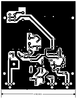
You can use the printed circuit designed by the author, which has plenty of space for both components as well as for the battery clip, space for this subject and the island left to screw the antenna. It is possible, but make a custom PCB with minimum space required, provided that you follow the guidelines of the electrical circuit. In both cases it is advisable to use printed circuit board in place of the phenolic pertinax since the latter absorbs moisture which would cause instability of the system.

Domestic TV Transmitter PCB1

Side tracks (welding) in size. (scale 1:1)

Domestic TV Transmitter PCB

Expanded components distribution.

Notes:
  • The 4.5MHz RF transformer (T1) can be anything that fits, provided you have the internal capacitor connected to the secondary.
  • L4 must be done manually. Respect the parameters given above.
  • If used in resistor R12, to be placed on the solder side of the printed circuit between the antenna output and ground. This component must be installed whenever you use an antenna other than the internal, making a correct fit between it and the circuit.
Adjust:

To calibrate the transmitter will need a TV receiver and a signal source such as a video recorder or a camcorder. Need, moreover, a non-metallic tool to adjust the coil L4 and the transformer T1. A new 9v battery can be used for adjustments, but if calibration is difficult, try doing it with a 12v power supply. Note that during the adjustment and testing of the unit, we find that it works much better with a stable supply filtered 12 volts. If you come to the same conclusion, add a voltage input connector welding it to the appropriate points on the circuit board (instead of the battery clip).

Tune the TV receiver in an unused channel (no transmission) between 2 and 6. The TV must be connected directly to the internal antenna, an external antenna or a cable system will not work. Make sure both knobs are in the center position (at halfway) and apply power to the circuit. Adjust L4 with non-metallic tool until the TV screen goes blank (rain disappears). Then, carefully adjust L4 to achieve the best possible reception. Connect the audio outputs of a VCR and other video source to J1 and J2, if necessary operate the VCR. You should see the image on the TV screen: if so, L4 setting up the best picture possible, and if not, check the circuit board in search of an error in welds or components in the inputs. Then adjust R3 for optimum brightness and R7 for a general adjustment of video quality. You may need to make minor adjustments on L4 after adjusting R3 and R7. Finally, adjust T1 with nonmetallic tool to get the best audio possible. After that the transmitter is properly calibrated.

Domestic TV Transmitter image
View completed and mounted equipment in your cabinet

Important:

The use of these systems is regulated by law in much of the world. Before operating, we suggest that you consult a competent legal authority on the scope and restrictions of the law regarding the use of these devices. In some countries can cause illegal emissions from confiscation of equipment to the prison of the copyright holder.


read more...

Signal Tracer and Injector

A simple test circuit to fault find audio and radio equipment. Can be used to inject a square wave signal, rich in harmonics, or used with headphones as an audio tracer.

Signal Tracer and Injector Circuit diagram


a single pole double throw sitch is used to switch between inject and trace modes. The diagram is drawn in trace mode, the earpiece being connected to the collector of the last transistor. Both transistors are wired as emitter followers, providing high gain. DC blocking is provided by the 1n capacitor at the probe end, and the two stages are capacitively coupled.

When the switch is thrown the opposite way (to the blue dot) both transistors are wired as an astable square wave generator. This provides enough harmonics from audio up to several hundred kilohertz and is useful for testing AM radio Receivers.
read more...

Simple 4 Channel Video Amplifier Using NJM2582

A very simple 4 channel video amplifier electronic circuit project can be designed using NJM2582 ic suitable for video applications with SCART connector . Design of the circuit is very simple and require few external electronic parts .

Simple 4 Channel Video Amplifier Circuit diagram


Some features of the NJM2582 are : Operating Voltage ±5V, +5V, +11V ; 6input 4output , 2input 1output Video SW , Internal LPF , 6dB Amplifier , Internal 75Ω Driver Circuit , DC output for SCART (FUNCTION SW, BLANKING) .
read more...
 
Copyright © 2019 W3circuits.blogspot.com • All Rights Reserved.
back to top