Showing posts with label Radio (RF). Show all posts

Simple Long-Range IR Transmitter

Most of the IR remotes work reliably within a range of 5 metres. The circuit complexity increases if you design a long range IR transmitter for reliable operation over a longer range, say, 10 metres. To double the range from 5 metres to 10 metres, you need to increase the transmitted power four times.

If you wish to realise a highly directional IR beam (very narrow beam), you can suitably use an IR laser pointer as the IR signal source. The laser pointer is readily available in the market. However, with a very narrow beam from the laser pointer, you have to take extra care, lest a small jerk to the gadget may change the beam orientation and cause loss of contact.

Long range IR transmitter

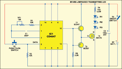
Here is a simple circuit that will give you a pretty long range. It uses three infrared transmitting LEDs (IR1 through IR3) in series to increase the radiated power. Further, to increase the directivity and so also the power density, you may assemble the IR LEDs inside the reflector of a torch.
long range IR transmitter
  
Fig. 1: Circuit of the long range IR transmitter
 
For increasing the circuit efficiency, a MOSFET (BS170) has been used, which acts as a switch and thus reduces the power loss that would result if a transistor were used. To avoid any dip during its ‘on’/‘off’ operations, a 100μF reservoir capacitor C2 is used across the battery supply. Its advantage will be more obvious when the IR transmitter is powered by ordinary batteries. Capacitor C2 supplies extra charge during ‘switching on’ operations.

As the MOSFET exhibits large capacitance across gate-source terminals, a special drive arrangement has been made using npn-pnp Darling ton pair of BC547 and BC557 (as emitter followers), to avoid distortion of the gate drive input. Data (CMOS-compatible) to be transmitted is used for modulating the 38 kHz frequency generated by CD4047 (IC1). However, in the circuit shown here, tactile switch S1 has been used for modulating and transmitting the IR signal.

Pin configurations
Fig. 2: Pin configurations of bc547/557 and bS170
 
Assemble the circuit on a general- purpose PCB. Use switch S2 for power ‘on’/‘off’ control. Commercially available IR receiver modules (e.g., TSOP1738) could be used for efficient reception of the transmitted IR signals.

Source by: EFY
read more...

Low-Cost 3 volts FM Transmitter

This very Simple Electronic Project and useful circuit diagram of an FM transmitter is sown in this schematic. This fm transmitter circuit is very simple and it has a acceptable transmission. The signal transited from this fm transmitter circuit can be received at almost 300 meters in open air The circuit require a 3volts operating voltage and can be tuned anywhere in the FM band.

Low-Cost 3 volts FM Transmitter Circuit Diagram:

FM Transmitter
 
You can use this rf transmitter circuit to transmit signal from your house to garden or from room to room . To listen the signal you can use any radio (portable or not ) that can work on FM band . The coil should be about 3mm in diameter and 5 turns. The wire is tinned copper wire, 0.61 mm in diameter.

After the coil in soldered into place spread the coils apart about 0.5 to 1mm so that they are not touching. If you don’t have a trim cap you can use a fixed value capacitor and you can vary the TX frequency by adjusting the spacing of the coils or placing a small piece of ferrite inside the coil, but the better way to change the transmission frequency is to use a variable capacitor.

Connect a half or quarter wavelength antenna (length of wire) to the aerial point. At an FM frequency of 100 MHz these lengths are 150 cm and 75 cm respectively. The calibration of this rf transmitter circuit is very simple and you need just to place a radio at some distance from the transmitter and set it somewhere about 89-90MHZ (chose the transmission frequency) and after that vary the transmitter oscillator frequency, by modifying the value of the capacitor. The transmission frequency is set to the desired frequency just when you can hear the transmitted signal.
read more...

Low-Cost 9V FM Transmitter

A very simple and useful circuit that require few external components and operates in FM band ( above 100 MHz ). This circuit diagram transmitter needs to be powered from a 9 volts battery or from another 9 volts regulated power supply . The tuned coil L1, has two output tappings for the antenna connection, marked "A" and "B". These are both low-level outputs and you choose which tapping you want to use ( stable low range, or more unstable but higher range).

Transmitter

Tap B (2.5%) takes just a very small portion of signal from the oscillator circuit and therefore gives a very frequency stable transmitter. The output level (around 2.5mW) and range are therefore somewhat reduced.  Tap A (10%) delivers very much more power (around 10mW) to the antenna load. This gives you a greater range, but at the expense of frequency stability.

All component leads should be kept as short as possible. The LINK wire on the PCB should lay flat on the PCB. Use the cutoff from a resistor leg. Antenna length for circuit diagram transmitter varies with frequency for optimum distance: 90MHz 80 cm, 95MHz 75cm, 100MHz 70 cm, 105 MHz 68 cm. The frequency determining elements (L1, C5 and C6) form a simple LC tuned oscillator. The inherent problem with this type of circuit diagram transmitter is that any external load (antenna) will change the operating frequency.

The inductor L1 must have around 5.5 turns of enameled 0.5 mm Cu wire , and must have a diameter ( coil diameter) around 5 mm.

read more...

Radio Beacon Converter

The radio beacon band extends from 280 to 516 kHz. Each beacon has its own characteristic AM`-modulated morse-coded callsign that is transmitted on a specific frequency. To be able to receive distant beacons, the aerial signal is passed through a band-pass filter that effectively suppresses longwave and mediumwave signals. 

Radio Beacon Converter Circuit Diagram:

Converter

The filter also converts the aerial impedance, Zm, from about 10 KOhmhm to the input impedance of mixer IC1, which is about 1 KOhmhm. The mixer adds or subtracts the received signal to/from the local oscillator signal so that the beacon signal can be received on a normal shortwave receiver. The resulting frequencies are from 9.72 to 9.48 MHz or from 10.280 to 10.516 MHz.

In the construction of the converter, some components must be surrounded by a metal shield, as indicated by dashed lines on the PC board layout. The circuit is aligned with the aid of an SSB receiver, to which the output of the converter is connected. Tune the receiver to 10 MHz and adjust the oscillator frequency of the converter with C8 for zero beat. Next, detune the receiver slightly until you hear a pleasant whistle, which is adjusted for minimum level with the aid of PI. Finally, tune to a beacon transmitting at or about 300 kHz and adjust C13 for maximum sound output.


read more...

Simple 9V FM Transmitter

This circuit diagram transmitter is a very simple and useful circuit that require few external components and operates in FM band ( above 100 MHz ). This circuit diagram transmitter needs to be powered from a 9 volts battery or from another 9 volts regulated power supply .

9V FM Transmitter Circuit Diagram:

FM Transmitter Circuit Diagram

The tuned coil L1, has two output tappings for the antenna connection, marked "A" and "B". These are both low-level outputs and you choose which tapping you want to use ( stable low range, or more unstable but higher range). Tap B (2.5%) takes just a very small portion of signal from the oscillator circuit and therefore gives a very frequency stable transmitter. The output level (around 2.5mW) and range are therefore somewhat reduced.

Tap A (10%) delivers very much more power (around 10mW) to the antenna load. This gives you a greater range, but at the expense of frequency stability. All component leads should be kept as short as possible. The LINK wire on the PCB should lay flat on the PCB. Use the cutoff from a resistor leg. Antenna length for circuit diagram transmitter varies with frequency for optimum distance: 90MHz 80 cm, 95MHz 75cm, 100MHz 70 cm, 105 MHz 68 cm.

The frequency determining elements (L1, C5 and C6) form a simple LC tuned oscillator. The inherent problem with this type of circuit diagram transmitter is that any external load (antenna) will change the operating frequency.


read more...

50MHz-300MHz Colpitts Oscillator

In this electronic project circuit you can see a very simple high efficiency Colpitts oscillator. In the higher frequency ranges, above 50 MHz, Colpitts oscillators are used because stray circuit capacitance will be in parallel with desired feedback capacitance and not cause undesirable spurious resonances that might occur with the tapped coil Hartley design. The FM VCO shown is a grounded base design with feedback from collector to emitter.

50MHz-300MHz Colpitts Oscillator Circuit Diagram:

Oscillator Circuit Diagram

A Colpitts oscillator is one of a number of designs for electronic oscillator circuits using the combination of an inductance with a capacitor for frequency determination. The distinguishing feature of the Colpitts oscillator circuit is that the feedback signal is taken from a voltage divider made by two capacitors in series. As you can see in the circuit diagram , this electronic project require few electronic parts an provide a 50 MHz-300MHz VCO with a tuning range of 2:1.

read more...

Micro Power AM Broadcast Transmitter

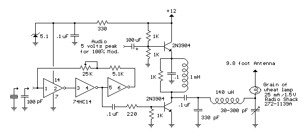
In this Electronic Circuit Project, a 74HC14 hex Schmitt trigger inverter is used as a square wave oscillator to drive a small signal transistor in a class C amplifier configuration. The oscillator frequency can be either fixed by a crystal or made adjustable (VFO) with a capacitor/resistor combination. A 100pF capacitor is used in place of the crystal for VFO operation.

Amplitude modulation is accomplished with a second transistor that controls the DC voltage to the output stage. The modulator stage is biased so that half the supply voltage or 6 volts is applied to the output stage with no modulation. The output stage is tuned and matched to the antenna with a standard variable 30-365 pF capacitor. Approximately 20 milliamps of current will flow in the antenna lead (at frequencies near the top of the band) when the output stage is optimally tuned to the oscillator frequency.

Micro Power AM Broadcast Transmitter Circuit Diagram:

AM Transmitter


A small 'grain of wheat' lamp is used to indicate antenna current and optimum settings. The 140 uH inductor was made using a 2 inch length of 7/8 inch (OD) PVC pipe wound with 120 turns of #28 copper wire. Best performance is obtained near the high end of the broadcast band (1.6 MHz) since the antenna length is only a very small fraction of a wavelength. Input power to the amplifier is less than 100 milliwatts and antenna length is 3 meters or less which complies with FCC rules.

Output power is somewhere in the 40 microwatt range and the signal can be heard approximately 80 feet. Radiated power output can be approximated by working out the antenna radiation resistance and multiplying by the antenna current squared. The radiation resistance for a dipole antenna less than 1/4 wavelength is R = 80*[(pi)^2]*[(Length/wavelength)^2]*(a factor depending on the form of the current distribution) The factor depending on the current distribution turns out to be [(average current along the rod)/(feed current)]^2 for short rods, which is 1/4 for a linearly-tapered current distribution falling to zero at the ends. Even if the rods are capped with plates, this factor cannot be larger than 1. Substituting values for a 9.8 foot dipole at a frequency of 1.6 MHz we get R= 790*.000354*.25 = .07 Ohms. And the resistance will be only half as much for a monopole or 0.035 Ohms. Radiated power at 20 milliamps works out to about I^2 * R = 14 microwatts.


read more...

Electronic Simple Project For Two Transistor AM Radio Receiver

Here is simple Electronic Circuit Project of two transistor AM radio receiver circuit. This two transistor AM radio circuit is also called “mini-radio”. It uses only 2 transistors and few passive components which makes is very easy to be constructed. Although the circuit is very simple, it functions very well without external antenna or ground connection. The transistor T1 works as a feedback regulated HF-amplifier and function as demodulator at the same time. The sensitivity of the receiver is dependent on the amount of feedback and can be adjusted by P1.

Two Transistor AM Radio Receiver Circuit Diagram:

Radio Circuit Diagram

The demodulated signal comes out from the collector of T1. The signal is then filtered by C3 so that only the audio signal will be amplified by T2. The amplified signal is then delivered to a high impedance “earphone”. The coil is 65 turns AM antenna wire around a 10 cm long x 10 mm diameter ferrite rod. The tap is at the fifth turn of the coil counting from its ground end. The coil must be installed as close as possible to the PCB.

PCB layout Circuit:

PCB layout

The sensitivity of the radio receiver can be greatly improved by attaching an external antenna into it. The external antenna must be coupled to the hot end of the coil through a 4.7 picofarad capacitor. The radio receiver cand be powered by a 9 volt battery. It consumes only 1 mA.

Parts Placement:

Parts


read more...

Simple and Small Active FM Amplifier

Simple and Small Active FM Amplifier With only a handfull of parts you can built this trusty FM Amplifier.

This amplifier will pull in all distant FM stations clearly. The circuit is configured as a common-emitter tuned RF pre-amplifier wired around VHF/UHF transistor Q1.

Active FM Amplifier Circuit Diagram

https://blogger.googleusercontent.com/img/b/R29vZ2xl/AVvXsEjnUwQN8YgV7baiY40nX0ChyphenhyphenOHGFe_eBHOHihBS5Emnj3j7sIhMTxP0C2-KgD8CkrI5dgUKUjPja-0U1XGKJ2Ha_7O7fgsA0qZ5daPCljon6kK3m0uFM7lOsD-5mGcZLOLGAAo9MD4R-ug/s1600/Active+FM+Amplifier+Circuit+Diagram.png

Parts List:
     R1 = 27K
     R2 = 270 ohm
     R3 = 1K

Tr1,Tr2 = 22pF, trimmer cap (15-40pF)
  C1,C2 = 5.6pF
     C3 = 0.001uF (1nF), ceramic
  C4,C5 = 0.01 (10nF), ceramic
     C6 = 0.1uF (100nF), ceramic

     Q1 = 2SC2498, 2SC2570, 2N5179, SK9139, or NTE10. NPN VHF/UHF transistor
     L1 = 4 turns of 20SWG magnet wire, 5mm diameter. (so-called 3T+1)
     L2 = 3 turns of 20SWG magnet wire, 5mm diameter.

All capacitors are ceramic, and 50V is the standard but the 25V types work fine too. Trimmer capacitors Tr1 and Tr2 (22pF) are adjusted for maximum gain. Input coil L1 consists of 4 turns of 20SWG enamelled copper wire over a 5mm diameter former. It is tapped at the first turn from the ground lead side. Coil L2 is similar to L1, but has only three turns. Pin configuration is shown in the diagram.


read more...

Simple 3 Volts FM Transmitter Schematic

This is a simple and useful circuit diagram of an FM transmitter is sown in this schematic . This FM Transmitter software is very simple and it has a acceptable transmission . The signal transited from this FM transmitter can be received at almost 300 meters in open air The circuit require a 3volts operating voltage and can be tuned anywhere in the FM band.

3V FM Transmitter Circuit Diagram

https://blogger.googleusercontent.com/img/b/R29vZ2xl/AVvXsEhlgyjwzfmjivDb4qagdm-eE-Af42l3zW2hohUpUEtIQmz8NzgtVD3UT-0o24BYn5dEnOm98-qmsX5INkVPToRz2yYH1JCb-Wl5UuLvx38jRzXjztIgsJh26msR_XvUWVCTDVpuUlRIleY/s1600/3+V+FM+TRANSMITTER+Circuit+Diagram.jpg

You can use this emitter circuit to transmit signal from your house to garden or from room to room . To listen the signal you can use any radio (portable or not ) that can work on FM band .

Connect a half or quarter wavelength antenna (length of wire) to the aerial point. At an FM frequency of 100 MHz these lengths are 150 cm and 75 cm respectively.

The calibration of this FM emitter circuit is very simple and you need just to place a radio at some distance from the transmitter and set it somewhere about 88-107MHZ( chose the transmission frequency ) and after that vary the transmitter oscillator frequency , by modifying the value of the capacitor . The transmission frequency is set to the desired frequency just when you can hear the transmitted signal.


read more...

How to build a Long-range FM Transmitter

How to build a Long-range FM Transmitter. The power output of most of these circuits is very low because no power amplifier stages were incorporated.

The transmitter circuit described here has an extra RF power amplifier stage, after the oscillator stage, to raise the power output to 200-250 milliwatts. With a good matching 50-ohm ground plane antenna or multi-element Yagi antenna, this transmitter can provide reasonably good signal strength up to a distance of about 2 kilometres.

Long-range FM Transmitter Circuit Diagram

FM Transmitter

The circuit built around transistor T1 (BF494) is a basic low-power variable-frequency VHF oscillator. A varicap diode circuit is included to change the frequency of the transmitter and to provide frequency modulation by audio signals. The output of the oscillator is about 50 milliwatts. Transistor T2 (2N3866) forms a VHF-class A power amplifier. It boosts the oscillator signals’ power four to five times. Thus, 200-250 milliwatts of power is generated at the collector of transistor T2.

For better results, assemble the circuit on a good-quality glass epoxy board and house the transmitter inside an aluminum case. Shield the oscillator stage using an aluminum sheet.

Coil winding details are given below:
L1 - 4 turns of 20 SWG wire close wound over 8mm diameter plastic former.
L2 - 2 turns of 24 SWG wire near top end of L1.
(Note: No core (i.e. air core) is used for the above coils)
L3 - 7 turns of 24 SWG wire close wound with 4mm diameter air core.
L4 - 7 turns of 24 SWG wire-wound on a ferrite bead (as choke)

Potentiometer VR1 is used to vary the fundamental frequency whereas potentiometer VR2 is used as power control. For hum-free operation, operate the transmitter on a 12V rechargeable battery pack of 10 x 1.2-volt Ni-Cd cells. Transistor T2 must be mounted on a heat sink. Do not switch on the transmitter without a matching antenna. Adjust both trimmers (VC1 and VC2) for maximum transmission power. Adjust potentiometer VR1 to set the fundamental frequency near 100 MHz.

This transmitter should only be used for educational purposes.


read more...

Easy Make a MP3 FM Transmitter

Easy make a MP3 FM Transmitter. Here's a simple VHF FM transmitter that could be used to play audio files from an MP3 player or computer on a standard VHF FM radio. The circuit use no coils that have to be wound. This FM transmitter can be used to listen to your own music throughout your home. When this FM transmitter used in the car, there is no need for a separate input to the car stereo to play back the music files from your MP3 player.

MP3 FM Transmitter Image 

USB FM Transmitter Image

To keep the circuit simple as well as compact, it was decided to use a chip made by Maxim Integrated Products, the MAX2606 [1]. This IC from the MAX2605-MAX2609 series has been specifically designed for low-noise RF applications with a fixed frequency. The VCO (Voltage Controlled Oscillator) in this IC uses a Colpitts oscillator circuit. The variable-capacitance (varicap) diode and feedback capacitors for the tuning have also been integrated on this chip, so that you only need an external inductor to fix the central oscillator frequency.

t is possible to fine-tune the frequency by varying the voltage to the varicap. Not much is demanded of the inductor, a type with a relatively low Q factor (35 to 40) is sufficient according to Maxim. The supply voltage to the IC should be between 2.7 and 5.5 V, the current consumption is between 2 and 4 mA. With values like these it seemed a good idea to supply the circuit with power from a USB port.

MP3 FM Transmitter Circuit Diagram

USB FM Transmitter
Parts List:

Resistors
(all SMD 0805)
R1,R2 = 22kΩ
R3 = 4kΩ7
R4,R5 = 1kΩ
R6 = 270Ω
P1 = 10kΩ preset, SMD (TS53YJ103MR10 Vishay Sfernice, Farnell # 1557933)
P2 = 100kΩ preset, SMD(TS53YJ104MR10 Vishay Sfernice, Farnell # 1557934)
Capacitors (all SMD 0805)
C1,C2,C5 = 4μF7 10V
C3,C8 = 100nF
C4,C7 = 2nF2
C6 = 470nF
Inductors
L1 = 390nF, SMD 1206 (LQH31HNR39K03L Murata, Farnell # 1515418)
L2 = 2200Ω @ 100MHz, SMD, common-mode choke, 1206 type(DLW31SN222SQ2L Murata, Farnell #1515599)
Semiconductors
IC1 = MAX2606EUT+, SMD SOT23-6 (Maxim Integrated Products)
Miscellaneous
K1 = 3.5mm stereo audio jack SMD (SJ1-3513-SMT
CUI Inc, DIGI-Key # CP1-3513SJCT-ND)
K2 = 5-pin header (only required in combination with 090305-I pre-emphasis circuit)
K3 = USB connector type A, SMD (2410 07 Lumberg, Farnell # 1308875)

A common-mode choke is connected in series with the USB connections in order to avoid interference between the circuit and the PC supply. There is not much else to the circuit. The stereo signal connected to K1 is combined via R1 and R2 and is then passed via volume control P1 to the Tune input of IC1, where it causes the carrier wave to be frequency modulated. Filter R6/C7 is used to restrict the bandwidth of the audio signal. The setting of the frequency (across the whole VHF FM broadcast band) is done with P2, which is connected to the 5 V supply voltage.

The PCB designed uses resistors and capacitors with 0805 SMD packaging. The size of the board is only 41.2 x 17.9 mm, which is practically dongle-sized. For the aerial an almost straight copper track has been placed at the edge of the board. In practice we achieved a range of about 6 metres (18 feet) with this. There is also room for a 5-way SIL header on the board. Here we find the inputs to the 3.5 mm jack plug, the input to P1 and the supply voltage. The latter permits the circuit to be powered independently from the mains supply, via for example three AA batteries or a Lithium button cell. Inductor L1 in the prototype is a type made by Murata that has a fairly high Q factor: minimum 60 at 100 MHz.

MP3 FM Transmitter PCB Layout 

FM Transmitter PCB Layout

Take care when you solder filter choke L2, since the connections on both sides are very close together. The supply voltage is connected to this, so make sure that you don’t short out the USB supply! Use a resistance meter to check that there is no short between the two supply connectors before connecting the circuit to a USB port on a computer or to the batteries.

P1 has the opposite effect to what you would expect (clockwise reduces the volume), because this made the board layout much easier. The deviation and audio bandwidth varies with the setting of P1. The maximum sensitivity of the audio input is fairly large. With P1 set to its maximum level, a stereo input of 10 mVrms is sufficient for the sound on the radio to remain clear. This also depends on the setting of the VCO. With a higher tuning voltage the input signal may be almost twice as large (see VCO tuning curve in the data sheet). Above that level some audible distortion becomes apparent. If the attenuation can’t be easily set by P1, you can increase the values of R1 and R2 without any problems.

Measurements with an RF analyzer showed that the third harmonic had a strong presence in the transmitted spectrum (about 10 dB below the fundamental frequency). This should really have been much lower. With a low-impedance source connected to both inputs the bandwidth varies from 13.1 kHz (P1 at maximum) to 57 kHz (with the wiper of P1 set to 1/10). In this circuit the pre-emphasis of the input is missing. Radios in Europe have a built-in de-emphasis network of 50 μs (75 μs in the US). The sound from the radio will therefore sound noticeably muffled. To correct this, and also to stop a stereo receiver from mistakenly reacting to a 19 kHz component in the audio signal, an enhancement circuit Is published elsewhere in this issue (Pre-emphasis for FM Transmitter, also with a PCB).

Notice:
The use of a VHF FM transmitter, even a low power device like the one described here, is subject to radio regulations and may not be legal in all countries.

read more...

How to Build a Fox Hunt Transmitter

It is a very Simple Build a Fox Hunt Transmitter. This 2 meter 144 MHz fox hunt transmitter is used in amateur competitions where a hidden transmitter is to be “hunted” using mostly home brewed receivers and antennas. The foxhunt electronic circuit is the transmitter. It radiates a high quality signal without unwanted harmonics. Transistor T1 and the crystal together make the oscillator that generates a 36MHz signal.

The unwanted 12MHz basic frequency of the oscillator is suppressed by the filter circuit made of L1, C3, C2. The L2/C4 circuit is set to the fourth harmonic or 144 MHz. The signal goes to the dual-gate-FET driver stage before finally radiating through the transmitting antenna. The output power is from 10…40mW. The radiated signal is also modulated by the gate circuit made of U1, U2, U3, U4. Gate U1 is a low frequency oscillator which generates a signal from 0.1 to 0.5Hz. This signal modulates the transmitter through the transistor T3.

Fox Hunt Transmitter Circuit Diagram

Transmitter

If the U1 output is “0″, transistor T3 is off and the transmitter is also off. On the other hand, if the U1 output is “1″, transistor T3 is on and the transmitter is on. During the “1″ period, gate U2 generates a square wave signal with a frequency form 0.1 to 1Hz. Gate U3 works as an inverter only. It determines whether gate U4 generates a 1KHz signal or not. A periodic burst signal is now present at the gate FET T2 to modulate the transmitter used at foxhunt.

Calibration of the foxhunt transmitter: Adjust the three trimmer capacitors to produse a maximum signal amplitude at the output.

Coil Data:
L1 = 470 nH
L2 is made of 5 windings of 0.8mm copper wire, 8 mm winding diameter. It is tapped at the first winding from the ground.

L3 is made of 0.8mm copper wire, 8mm winding diameter, 3 windings at the FET side and 2 windings at the antenna side. Adjust the coupling between the two windings sides to get a maximum signal output amplitude.
The circuit can be powered with a 9 volt battery. It consumes around 20mA only.

Fox Hunt Transmitter Active Components.

T1 = 2SA256
T2 = 3N205
U1, U2, U3, U4 = IC1 = 4093


read more...

How to Build a 18w FM Transmitter

Build a 18w FM Transmitter. Here's a transmitter for commercial FM band provides up to 18 watts of power. Entering an audio signal 1 Vpp standard , which may come from a mixer or stereo coding stage , this system can cover an entire medium of low houses people or an entire neighborhood in a city. If required you can build more power and interconnect output stages to increase the coverage area of the station. 

Since the electronic diagram is too wide for placement on screen we decided segregated into two , in order to be seen without the need to move from side to side of the screen. The point where we cut only two drivers ( represented by A and B ) which are marked with arrows.

FM Transmitter


18w FM Transmitter
 
 See the Complete Circuit Diagram

  
The Coils and Shocks Should Be Made According to the Following Table:

L1 ------- 3 Turns on ferrite of 5x10mm
L2 ------- 3 Turns on air 9mm ( 10mm long )
L3 ------- 1 Return on 12mm air
L4 ------- 4 turns on air 9mm ( 12mm long )
L5 ------- 2.5 laps on ferrite of 5x10mm
L6 ------- 1 Return on 12mm air
L7 ------- 2.5 laps on HF type ferrite 10x5mm
L8 ------- 3 Turns on air L8 9mm ( 8mm long )
L9 ------- 1 Return on 12mm air
L10 ------- 2.5 laps on ferrite of 5x10mm
L11 ------- 2.5 laps on ferrite of 5x10mm
L12 ------- 7 laps on air 9mm ( 19mm long )
L13 ------- 3 Turns on air L13 13mm ( 7mm long )
 

The variable capacitor connected to the collector of transistor BF199 to adjust the transmission frequency of the circuit. 2K2 potentiometer (which is linear ) serves fine tuning. Once the output frequency should be adjusted following variable capacitors to calibrate the remaining stages of the transmitter. Remember that these settings are made from the capacitor on the left to the one on the right. Remember that the initial settings should accomplish with phantom loads and not the ultimate antenna to avoid interference to other stations.

With respect to the feeding circuit 14V and 2.5A provides 15W , whereas 18V and 3.5A provides 18W, in all cases the source must be stabilized.

The circuit must be built on an epoxy printed with the upper face (components ) reserved for interconnecting tracks and the bottom (solder ) to the ground plane. We have no printed circuit design . If someone builds this transmitter would appreciate email send us the design of the board. 

Transistors 2N3924 , 2N4427 and BLY88 must be mounted heatsinks . In this type of components used sinks star-shaped circular . In the case of transistors 2Nxxxx the ideal size is 20mm in diameter and 10mm in height, while for the BLY88 must be 75mm diameter by 100mm tall. It is mandatory to use silicone grease to optimize the transfer of temperature of the transistors to their sinks . Remember that excessive heat (a part of the output instability ) can cause damage to components.

read more...

1W Shortwave Transmitter

While it may sound a watt insufficient to transmit radio signals , shortwave something special happen . Considering that a station as RPI ( Pirate Radio International ) , which broadcasts from the Andes ( the mast was spared the boys! ) Has a 100-watt transmitter on a J -Pole antenna type and with that power comes Russia and even China came to the conclusion that we can cover our modest quietly watt city where we mount .

1W Shortwave Transmitter Circuit Diagram

Transmitter Circuit Diagram

But we must not forget that no matter the radiated power , if our system is deficient antenna will not reach the next block . So pay attention to the type and size of antenna to use . An alternative is to build dipoles , which although large , work quite well .

Here is the electronic design of the transmitter, which we thank New Zealand station . As seen , there are a handful of passive components , two transformers , inductors and a pair of low-power transistors . The circuit is powered by 13.8vy consumes about 3 watts . In the construction of this project, take into account some aspects :
  • The temperature is crucial for the stability of the system, if the transistors overheat the output frequency can be unstable .
  • The crystal oscillator must be chosen according to the desired transmit frequency .
  • The printed circuit which will be reinforced epoxy . If using risk phenolic moisture to condense inside and make capacitance effect , altering the operation.
  • The source must be stabilized as much as possible to avoid frequency shifts .
  • The inductors should be as accurate as possible as these are calculated for optimum results.
  • If the power source is removed physically from the transmitter is advisable 100nF capacitors placed at the ends of the wire to prevent noise transmission seizes .
Once armed the system would be placed in a suitable enclosure , if metal is better. The output to the antenna is done with a conventional keg type connector . Do not use power and audio connectors . The coaxial cable to the radiant should be adequate for this type of installation. A poor wiring can reduce the final power radiated .

An out-band antenna used to increase ROE equipment, causing losses to the radiated power .

After this you need to enter the audio terminals with a modulation signal (one TDA2002 perfectly fulfills that role ) and start broadcasting in the fascinating world of Shortwave.

Remember that this type of activity is (or at least should be ) regulated by the state. Sure on the legal aspects before transmitting. According to the laws of the place where the emissions perform , we may remove the equipment and radiant . Be careful .


read more...

Stereo FM Transmitter Using BA1404

This circuit , whose only active component is an integrated circuit , to listen to your radio walkman headband or the signal from a computer, a stereo TV or hi-fi . It has excellent signal to noise ratio , very good channel separation is easy to adjust and the range is more than adequate for home use. Another possible use is in the car to enter the vehicle's stereo signal a Discman or MP3 player even when the team does not have line inputs , simply tune the transmitter on a free position and ready .

Stereo FM Transmitter Circuit Diagram


FM Transmitter Circuit Diagram


As you can see the circuit is very simple. The incoming stereo audio signal is conditioned and leveled by a handful of resistors and capacitors and then enter the integrated circuit . Other components are responsible for the generation of a pilot signal, the signal combination to achieve the MPX and the output buffer to the antenna.

The circuit operates at 3V . If powered with any voltage than directed will destroy the IC. The antenna may be a wire rod or 60cm long telescopic FM antenna . The signal input operates in the millivolt range and can attach knobs to adjust the audio level.

First tunes into a radio ( preferably digital and good quality ) dial a position where there is no broadcasting station . Then Turn On the transmitter and turning the trimmer 47pF , tune the transmitter so that the audio signal at the inputs is heard in the receiver. When you get the strongest signal possible to adjust the 50K preset until the stereo station indicator lights on your receiver . If the input signal is too strong ( it shows when the receiver is distorted ) will be convenient to put knobs on the transmitter input to lower the sensitivity.

The coil in parallel with the trimmer 47pF is formed by three turns of wire on a 0.5mm 5mm ferrite core .


read more...

Simple RF Amplifier

This circuit is useful in the amplification of small signals. The gain will vary with frequency, the data obtained from it were obtained with a frequency of 2.5 Mhz.

Simple RF Amplifier Circuit Diagram

RF amplifier Circuit Diagram


This circuit was tested with frequencies between 500kHz to lOMhz. It can be used as a preamplifier circuit for receiving MW (medium wave).


read more...

Power amp (10 w) for FM Transmitter

This amplifier increases the power of an FM transmitter 50 mW to 10 W in the range 88 to 108 MHz

Power amp (10 w) for FM Transmitter Circuit Diagram

FM Transmitter Circuit Diagram

FM Transmitter


It is quite critical assembly and RF power transistors must be mounted on heat radiators and handled with utmost care.

The coil L1 is formed by 04 turns of wire of 1 mm in diameter in the form of 8 mm diameter. The coil L5 is formed of 07 turns of wire 0.5 cm in diameter in the form of 6 mm in diameter, the coil L6 is wound wire of 1 mm and consists of 03 turns in the form of 10 mm diameter. Finally coil L2 consists of 04 turns of wire of 1 mm diameter in the shape of 10 mm.

The transformer T1 includes coils L2, L3 and L4, and these coils has turns of one wire of 0.5 mm figure 2. In this same figure we have to identify the terminals of the transistors. The capacitors must be ceramic disk type or plateau and resistors are 1/4 W.


read more...

Portable and Low Power VHF FM Transmitter

This electronic circuit is a simple VHF FM transmitter circuit. The circuit can easily make portable use for a small 9 volt battery. Transmitter range from 60 to 100 meters range.  The construction of the circuit is very simple.
  • Electrically adjustable frequency between 88 and 108MHz.
  • Portable and low power consumption.
  • You can use any FM receiver.
  • 9 Volt works.
Portable and Low Power VHF FM Transmitter Circuit Diagram

FM Transmitter Circuit Diagram
Parts list:
R1 = 10K
R2 = 15K
R3 = 3.3K
R4 = 470 ohm
R5 = 100K
R6 = 4.7K
VR 1 = 10K Pot meters

VALUE
C1 = 0.1uF----- 104
C2 = 0.001uF---- 102
C3 = 0.0015uF---- 152
C4 = 10pF ----- 10
C5 = 3pfF ----- 3
C6 = 2.5pF----- 2.5
C7 = 10pF ----- 10
C8 = 0.01uF---- 103
C9 = 0.022uF----- 223
C10 = 1pF ----- 1
C11 = 0.001uF---- 102

read more...

Use A DAC To Bias Your Varactor Diode

Varactor (or “varicap”) diodes are used primarily in radio-frequency (RF) circuits to provide a capacitance that can be varied by changing the applied voltage. These types of diodes often are used for tuning circuits, such as RF oscillators and filters found in wireless applications like wireless microphones and radios. Designers, then, should know about the benefits of using a nonvolatile digital-to-analog converter (DAC) to provide the biasing voltage of a varactor diode used as a voltage-controlled capacitor.

The varactor diode is operated under reverse bias, which creates a depletion zone around the P-N junction. Changing the level of the reverse bias changes the thickness of the depletion region and, thus, the effective capacitance of the diode. Increasing voltage causes a decrease in capacitance.

Varactor diodes are specified with a nominal capacitance value and the range of capacitance that can be achieved with a maximum and minimum voltage level. Increasing the bias voltage range increases the capacitance range available, but designers can also look for varactors with a larger capacitance- to-voltage ratio.

A convenient solution for creating a varying bias voltage is to use a DAC. Most DACs have an output voltage range of 0 V to +5.5 V. If a higher voltage bias is required, though, then a high-voltage DAC can be used. However, it may be more cost-effective to use a low-cost, high-voltage operational amplifier in a non-inverting configuration to provide level shifting of the output voltage from a common 5.5-V DAC.

 
The LC-tank circuit portion of a voltage-controlled oscillator allows for FM modulation in wireless microphones and radios. Its back-to-back varactor configuration minimizes the effects of RF modulation.

Using a DAC does introduce sources of potential error. The varactor is affected by any form of amplitude variation of the bias voltage, resulting in an undesired shift in capacitance. Deterministic errors can be accounted for when using the microcontroller to program the DAC output voltage. The primary sources of error that should be considered include varactor nonlinearity, offset errors, and DAC integral nonlinearity (INL). RF modulation may also be caused by voltage induced from a noise source – perhaps from an antenna in the system. The figure shows an LC-tank circuit portion of a voltage-controlled oscillator. This circuit allows for FM modulation in the aforementioned wireless microphone or radio.

Here, a back-to-back varactor configuration minimizes the effects of RF modulation. If a varying signal is injected, the bias across one diode increases as the other decreases, keeping overall capacitance unchanged. Note that the two diodes are in series with each other, so capacitance is half of a single varactor setup.

To also prevent RF signals from affecting the circuitry outside the tuning circuit, the bias voltage is fed through an isolation resistor or an RF choke. There are other benefits to using a DAC to bias a varactor diode. For example, multiple-output-channel DAC devices can be used in a multistage application. Additionally, in a four-channel DAC, three channels could potentially be used for separate band-pass filters for low-, mid-, and high-frequency filtering. The fourth output could be used for offset voltage calibration elsewhere in the circuit, or it could be turned off when it isn’t in use. Space and design time can be saved by avoiding having to set up separate biasing schemes.

Some DACs, such as the MCP4728, also offer on-board nonvolatile memory, which can store configuration data such as output-voltage levels and channel status (on/off). This enables the device to be reset or powered up into a known set state, which could allow a pre-programmed tune to be stored. The tune could be recalled when a desired event or input occurs or when power is lost and restored.
read more...
 
Copyright © 2019 W3circuits.blogspot.com • All Rights Reserved.
back to top