How to Build a UPS for USB devices

Portable systems often include circuitry that derives power from an external source, such as USB. When the system disconnects from the USB supply, a battery takes over and supplies current via a dc/dc converter. A diode-OR connection (Figure 1 offers the easiest way to ensure that the supply voltage doesn't sag during this switchover to the battery. The diode's forward voltage drop, however, can reduce battery life and efficiency.
 
Build a UPS for USB devices

A diode-OR connection is effective but lossy.


Computer Related
 A boost-converter circuit is an improvement over the simple diode-OR connection.

The single-cell, boost-converter circuit with external PFET (Figure 2) is an improvement over the diode-OR connection. The PFET, Q1, coupled with IC1's internal gain block, forms a linear regulator. The USB power supply has a diode-OR connection to Q1's source. Setting the boost converter's output to 3.4V allows the drain of Q1 to regulate to 3.3V. This configuration produces negligible loss in Q1. The bus-supply voltage available to USB devices ranges from 4.4 to 5.25V.

When you connect the bus, it forward-biases D1 and causes the boost converter to idle. The converter continues to idle as long as its output remains above the 3.4V regulation point. The bus supply serves the load and activates the current source to charge the battery.

Computer Related
These waveforms (bottom trace, load voltage) show that the load current suffers no interruption during a switchover from USB to battery.

Adjusting R1 allows you to set the current-source output to charge the nickel-metal-hydride cells at a level one-tenth the battery's capacity. Disconnecting the circuit from the USB supply causes the boost converter to cease idling and supply current to the load via the battery. Figure 3 shows that the load current suffers no interruption during a switchover from USB to battery.


read more...

Digital But Simple Electronic Lock

The digital lock shown below uses 4 common logic ICs to allow controlling a relay by entering a 4 digit number on a keypad. The first 4 outputs from the CD4017 decade counter (pins 3,2,4,7) are gated together with 4 digits from a keypad so that as the keys are depressed in the correct order, the counter will advance.

As each correct key is pressed, a low level appears at the output of the dual NAND gate producing a high level at the output of the 8 input NAND at pin 13. The momentary high level from pin 13 activates a one shot circuit which applies an approximate 80 millisecond positive going pulse to the clock line (pin 14) of the decade counter which advances it one count on the rising edge.

Digital But Simple Electronic Lock Circuit Diagram

Electronic Lock Circuit Diagram


A second monostable, one shot circuit is used to generate an approximate 40 millisecond positive going pulse which is applied to the common point of the keypad so that the appropriate NAND gate will see two logic high levels when the correct key is pressed (one from the counter and the other from the key). The inverted clock pulse (negative going) at pin 12 of the 74C14 and the positive going keypad pulse at pin 6 are gated together using two diodes as an AND gate (shown in lower right corner). The output at the junction of the diodes will be positive in the event a wrong key is pressed and will reset the counter.

When a correct key is pressed, outputs will be present from both monostable circuits (clock and keypad) causing the reset line to remain low and allowing the counter to advance. However, since the keypad pulse begins slightly before the clock, a 0.1uF capacitor is connected to the reset line to delay the reset until the inverted clock arrives. The values are not critical and various other timing schemes could be used but the clock signal should be slightly longer than the keypad pulse so that the clock signal can mask out the keypad and avoid resetting the counter in the event the clock pulse ends before the keypad pulse.

The fifth output of the counter is on pin 10, so that after four correct key entries have been made, pin 10 will move to a high level and can be used to activate a relay, illuminate an LED, ect. At this point, the lock can be reset simply by pressing any key.

The circuit can be extended with additional gates (one more CD4011) to accept up to a 8 digit code. The 4017 counting order is 3 2 4 7 10 1 5 6 9 11 so that the first 8 outputs are connected to the NAND gates and pin 9 would be used to drive the relay or light. The 4 additional NAND gate outputs would connect to the 4 remaining inputs of the CD4068 (pins 9,10,11,12). The circuit will operate from 3 to 12 volts on 4000 series CMOS but only 6 volts or less if 74HC parts are used. The circuit draws very little current (about 165 microamps) so it could be powered for several months on 4 AA batteries assuming only intermittent use of the relay.


read more...

32 Watt Amplifier Using by TDA2050V

A 32 Watt per channel stereo power amplifier made using the TDA2050V monolithic integrated circuit.

32 Watt Amplifier Circuit Diagram

Amplifier Circuit Diagram

Notes:

This circuit is for a 32 Watt stereo audio power amplifier using the TDA20501. With a dual 22 Volt supply this amplifier can deliver 32W into 8 ohm loudspeakers. Moreover, the TDA 2050 delivers typically 50W music power into 4 ohm load over 1 sec at VS= 22.5V and f = 1KHz. The amplifier is cased as a Pentawatt package see pinout below:

TDA2050V

This is a power amplifier and requires 200mV RMS for full output. Voltage gain is 30.5dB with resistor values shown. Closed loop gain is set by Ratio R1/R2. Increase R2 for less gain and vice versa. Power bandwidth is 20Hz to 80KHz. R3, C3 and R6, C11 form a zobel network to prevent high frequency instability.

The speaker is direct coupled, therefore no expensive large value electrolytics are needed and the bass will be crisp and clean. It is advisable to place fuses in the power supply (not shown).

Parts List:

R1,R4,R5,R8______22k 1/4W Resistor
R2,R7__________680R 1/4W Resistor
R3,R6___________2.2R 1/4W Resistor
C1,C10___________1u NP 25V Capacitor
C2,C12__________22u 63V Electrolytic
C3,C11_________0.47u 400V Polyester
C4,C7,C8,C9_____100n 400V Polyester
C5,C6,C13,C14___220u 63V Electrolytic
U1,U2__________TDA2050V 32W Audio Power Amp


read more...

How to Build AC Line Current Detector

This circuit will detect AC line currents of about 250 mA or more without making any electrical connections to the line. Current is detected by passing one of the AC lines through an inductive pickup (L1) made with a 1 inch diameter U-bolt wound with 800 turns of #30 - #35 magnet wire. The pickup could be made from other iron type rings or transformer cores that allows enough space to pass one of the AC lines through the center. 

Only one of the current carrying lines, either the line or the neutral should be put through the center of the pickup to avoid the fields cancelling. I tested the circuit using a 2 wire extension cord which I had separated the twin wires a small distance with an exacto knife to allow the U-bolt to encircle only one wire.

AC Line Current Detector Circuit Diagram

Detector Circuit Diagram

The magnetic pickup (U-bolt) produces about 4 millivolts peak for a AC line current of 250 mA, or AC load of around 30 watts. The signal from the pickup is raised about 200 times at the output of the op-amp pin 1 which is then peak detected by the capacitor and diode connected to pin 1. The second op-amp is used as a comparator which detects a voltage rise greater than the diode drop. The minimum signal needed to cause the comparator stage output to switch positive is around 800 mV peak which corresponds to about a 30 watt load on the AC line.

The output 1458 op-amp will only swing within a couple volts of ground so a voltage divider (1K/470) is used to reduce the no-signal voltage to about 0.7 volts. An additional diode is added in series with the transistor base to ensure it turns off when the op-amp voltage is 2 volts. You may get a little bit of relay chatter if the AC load is close to the switching point so a larger load of 50 watts or more is recommended. The sensitivity could be increased by adding more turns to the pickup.

read more...

Flashing LED Battery Status Indicator

A Battery-status Indicator circuit can be useful, mainly to monitor portable Test-gear instruments and similar devices. LED D1 flashes to attire the user's attention, signaling that the circuit is running, so it will not be left on by mistake. The circuit generates about two LED flashes per second, but the mean current drawing will be about 200µA. Transistors Q1 and Q2 are wired as an uncommon complementary astable multivibrator: both are off 99% of the time, saturating only when the LED illuminates, thus contributing to keep very low current consumption.

Flashing LED Battery Status Indicator Circuit Diagram

Indicator Circuit Diagram


The circuit will work with battery supply voltages in the 5 - 12V range and the LED flashing can be stopped at the desired battery voltage (comprised in the 4.8 - 9V value) by adjusting Trimmer R4. This range can be modified by changing R3 and/or R4 value slightly.

When the battery voltage approaches the exhausting value, the LED flashing frequency will fall suddenly to alert the user. Obviously, when the battery voltage has fallen below this value, the LED will remain permanently off.

To keep stable the exhausting voltage value, diode D1 was added to compensate Q1 Base-Emitter junction changes in temperature. The use of a Schottky-barrier device (e.g. BAT46, 1N5819 and the like) for D1 is mandatory: the circuit will not work if a common silicon diode like the 1N4148 is used in its place.

Note:

Mean current drawing of the circuit can be reduced further on by raising R1, R7 and R9 values.
read more...

How to Build a Shake Tic Tac LED Torch

In the diagram, it looks like the coils sit on the “table” while the magnet has its edge on the table. This is just a diagram to show how the parts are connected. The coils actually sit flat against the slide (against the side of the magnet) as shown in the diagram:

Shake Tic Tac LED Torch Circuit Diagram

LED Torch Circuit Diagram

The output voltage depends on how quickly the magnet passes from one end of the slide to the other. That's why a rapid shaking produces a higher voltage. You must get the end of the magnet to fully pass though the coil so the voltage will be a maximum. That’s why the slide extends past the coils at the top and bottom of the diagram.

The circuit consists of two 600-turn coils in series, driving a voltage doubler. Each coil produces a positive and negative pulse, each time the magnet passes from one end of the slide to the other.

The positive pulse charges the top electrolytic via the top diode and the negative pulse charges the lower
electrolytic, via the lower diode.

The voltage across each electrolytic is combined to produce a voltage for the white LED. When the combined voltage is greater than 3.2v, the LED illuminates. The electrostatics help to keep the LED illuminated while the magnet starts to make another pass.


read more...

1W Shortwave Transmitter

While it may sound a watt insufficient to transmit radio signals , shortwave something special happen . Considering that a station as RPI ( Pirate Radio International ) , which broadcasts from the Andes ( the mast was spared the boys! ) Has a 100-watt transmitter on a J -Pole antenna type and with that power comes Russia and even China came to the conclusion that we can cover our modest quietly watt city where we mount .

1W Shortwave Transmitter Circuit Diagram

Transmitter Circuit Diagram

But we must not forget that no matter the radiated power , if our system is deficient antenna will not reach the next block . So pay attention to the type and size of antenna to use . An alternative is to build dipoles , which although large , work quite well .

Here is the electronic design of the transmitter, which we thank New Zealand station . As seen , there are a handful of passive components , two transformers , inductors and a pair of low-power transistors . The circuit is powered by 13.8vy consumes about 3 watts . In the construction of this project, take into account some aspects :
  • The temperature is crucial for the stability of the system, if the transistors overheat the output frequency can be unstable .
  • The crystal oscillator must be chosen according to the desired transmit frequency .
  • The printed circuit which will be reinforced epoxy . If using risk phenolic moisture to condense inside and make capacitance effect , altering the operation.
  • The source must be stabilized as much as possible to avoid frequency shifts .
  • The inductors should be as accurate as possible as these are calculated for optimum results.
  • If the power source is removed physically from the transmitter is advisable 100nF capacitors placed at the ends of the wire to prevent noise transmission seizes .
Once armed the system would be placed in a suitable enclosure , if metal is better. The output to the antenna is done with a conventional keg type connector . Do not use power and audio connectors . The coaxial cable to the radiant should be adequate for this type of installation. A poor wiring can reduce the final power radiated .

An out-band antenna used to increase ROE equipment, causing losses to the radiated power .

After this you need to enter the audio terminals with a modulation signal (one TDA2002 perfectly fulfills that role ) and start broadcasting in the fascinating world of Shortwave.

Remember that this type of activity is (or at least should be ) regulated by the state. Sure on the legal aspects before transmitting. According to the laws of the place where the emissions perform , we may remove the equipment and radiant . Be careful .


read more...

How to Create a Alarm Using 4-Buttons

To open the lock, buttons S1, S2, S3, and S4 must be pressed in this order. They must be pressed for more than 0.7 seconds and less than 1.3 seconds.

Alarm Using 4-Buttons Circuit Diagram

Alarm Circuit Diagram

Reset button S5 and disable button S6 are also included with the other buttons and if the disable button is pressed, the circuit will not accept any code for 60 seconds. Each of the 3v3 zeners can be replaced with two red LEDs and this will show how you are progressing through the code. Make sure the LEDs are not visible to other users.


read more...

Stereo FM Transmitter Using BA1404

This circuit , whose only active component is an integrated circuit , to listen to your radio walkman headband or the signal from a computer, a stereo TV or hi-fi . It has excellent signal to noise ratio , very good channel separation is easy to adjust and the range is more than adequate for home use. Another possible use is in the car to enter the vehicle's stereo signal a Discman or MP3 player even when the team does not have line inputs , simply tune the transmitter on a free position and ready .

Stereo FM Transmitter Circuit Diagram


FM Transmitter Circuit Diagram


As you can see the circuit is very simple. The incoming stereo audio signal is conditioned and leveled by a handful of resistors and capacitors and then enter the integrated circuit . Other components are responsible for the generation of a pilot signal, the signal combination to achieve the MPX and the output buffer to the antenna.

The circuit operates at 3V . If powered with any voltage than directed will destroy the IC. The antenna may be a wire rod or 60cm long telescopic FM antenna . The signal input operates in the millivolt range and can attach knobs to adjust the audio level.

First tunes into a radio ( preferably digital and good quality ) dial a position where there is no broadcasting station . Then Turn On the transmitter and turning the trimmer 47pF , tune the transmitter so that the audio signal at the inputs is heard in the receiver. When you get the strongest signal possible to adjust the 50K preset until the stereo station indicator lights on your receiver . If the input signal is too strong ( it shows when the receiver is distorted ) will be convenient to put knobs on the transmitter input to lower the sensitivity.

The coil in parallel with the trimmer 47pF is formed by three turns of wire on a 0.5mm 5mm ferrite core .


read more...

How to Make a Transistor Tester

The 555 operates at 2Hz. Output pin 3 drives the circuit with a positive then zero voltage. The other end of the circuit is connected to a voltage divider with the mid-point at approx 4.5v. This allows the red and green LEDs to alternately flash when no transistor is connected to the tester.

TransistorTester Circuit Diagram

Tester Circuit Diagram

If a good transistor is connected, it will produce a short across the LED pair when the voltage is in one direction and only one LED will flash. If the transistor is open, both LED’s will flash and if the transistor is shorted, neither LED will flash.


read more...

Light Detector Using 555IC

This circuit detects light falling on the Photo-cell (Light Dependent Resistor) to turn on the 555 and create a tone that is delivered to the speaker. Pin 4 must be held below 0.7v to turn the 555 off. Any voltage above 0.7v will activate the circuit. The adjustable sensitivity control is needed to set the level at which the circuit is activated. 

Light Detector Circuit Diagram

Detector Circuit Diagram

When the sensitivity pot is turned so that it has the lowest resistance (as shown in red), a large amount of light must be detected by the LDR for its resistance to be low. This produces a voltage-divider made up of the LDR and 4k7 resistor. As the resistance of the LDR decreases, the voltage across the 4k7 increases and the circuit is activated.

When the sensitivity control is taken to the 0v rail, its resistance increases and this effectively adds resistance to the 4k7. The lower-part of the voltage-divider now has a larger resistance and this is in series with the LDR. Less light is needed on the LDR for it to raise the voltage on pin 4 to turn the 555 on.


read more...

8 Random Flashing LEDs using 555timer

This project flashes eight LEDs in an apparently random manner. It uses a 4060 combined counter and display driver IC which is designed for driving 7-segment LED displays.

8 Random Flashing LEDs Circuit Diagram


Flashing LEDs Circuit Diagram

The sequence is not really random because seven of the LEDs would normally be the display segments, the eighth LED is driven by an output that is normally used for driving further counters. The table below shows the sequence for the LEDs. You can use less than eight LEDs if you wish and the table may help you decide which ones to use for your purpose. Source

read more...

Buck IC Boosts Battery Voltage for White LED

 White-light LEDs are finding their way into many markets that incandescent bulbs once served. Flashlights are among the newer applications in which reliability, ruggedness, and ability to control the power draw of the LEDs make these devices attractive. With incandescent bulbs, the power management for the device is a simple on-off switch. However, the LEDs cannot operate directly from the two cells you typically find in most flashlights, because their required voltage is 2.8 to 4V, compared with a battery voltage of 1.8 to 3V.

The power management has a further complication because the light output of the LED relates to current, and the LED's characteristics are extremely nonlinear with voltage. One approach to this problem is to boost the power supply with a current limit. A number of devices for LED applications are available; however, their current ratings are typically too low for the 1 to 5W that flashlight applications need.

Buck IC Boosts Battery Voltage for White LED Circuit Diagram

White LED

Figure 1 presents an alternative to the typical boost power regulator. A buck-converter IC, IC1, generates the higher voltage that the white-light LED needs. An internal buck power stage connects between VIN and PGND, sourcing current to output Pin L. This circuit operates by turning on the high switch, thereby connecting the battery voltage across inductor L1. Once inductor L1 stores sufficient energy, the high-side switch turns off. The inductor current drives the switching node negative, and energy transfers through the low side into output capacitor C1, creating an essentially lossless switching event. Also, because the high- and low-side switches are MOSFETs, voltage drop is lower than that of a diode implementation; therefore, efficiency can be high.

The converter IC monitors the current through the LED via a current-sense resistor and compares the current-sense voltage with an internal 0.45V reference within the converter IC to achieve regulation. Current and, therefore, illumination are functions of the current-sense resistor voltage. Although the internal reference voltage of the IC is lower than that of most other ICs, it does cause an appreciable power loss. With the LED voltage of 2.8 to 4V, it degrades efficiency by 10 to 14%. Reducing the resistor's value and using an amplifier to sense the current at a lower voltage could reduce this loss.

White LED Circuit Diagram

Figure 2 shows load-current regulation and boost voltage at a 350-mA current setpoint. Efficiency is 80% or better over the normal battery-voltage range but falls as battery voltage drops to end-of-life values. Also, the figure shows the impact of the resistive-current sensing. At high input voltages, the efficiency approaches 95%, and, at low input voltages, it falls to 80%. The trend for the curves stems from two interrelated effects: At high input voltage, input current and, hence, switch current are low. Therefore, conduction and switching losses are low. Second, much like an autotransformer, the boost power stage does not handle the total output power.

The amount of power that the power stage handles relates to the boost voltage, or the difference between the input voltage and the LED voltage. In this design, the LED voltage is approximately 3.7V, so that at high line of 3.2V, the power stage handles only 13% ((3.7–3.2)/3.7) of the power. At low line, in which the currents are much higher, the power stage handles almost four times as much, or 50%, of the power. Although a buck controller is not an obvious choice for this application, it provides low-cost, low-input-voltage operation and good efficiency over a wide input-voltage variation. Source


read more...

Auto LED Taillight for a Bike

This is a circuit for automatically switching off and LED taillight for a bike. The backlight turns on by movement (in the dark). After about 20 minutes of inactivity, the backlight is switched off again. So you cannot forget to turn off the backlight so that you are less likely surprised by batteries. 

Auto LED Taillight Circuit Diagram

Auto LED Circuit Diagram

S1 is a motion switch. When the switch closes C1 is charged. Therefore FET switches T1 and burn the LED. T1 can however only enabled when R3 is sufficiently high resistance, or when it is dark. R1 C1 discharge slowly so that after about 20 minutes the FET turns off and the LED goes out.

The circuit may be built into the housing of a rear light on the battery that is inexpensive to buy in the market. That way you already have a beautiful body.

Parts List:

     R1 = 2.2 MΩ
     R2 = 2,2 kohm
     R3 = LDR
     R4 = 220 K?
     R5 = 22 K?
     R6 = 220 Ω
     C1 = 100 V μF/16
     D1 = high intensity LED 5mm red
     T1 = BS170
     S1 = motion switch (eg RS No. 455-3671)
     S2 = switch

read more...

220 V Thermostats Schematic

This is a universal thermostat, which can be used to switch. Used 220 V The author uses the circuit as a breeding thermostat.

220 V Thermostats Circuit Diagram:
 

The circuit is built around an opamp 741, which is the voltage of the voltage divider R1/R2/R3 compares with the reference voltage of R4/R5/P1. As the temperature rises, the resistance of the NTC fall's, causing the voltage drops to the positive input of the opamp. At some point the folded opamp to spert and the transistor T1 and the load is switched off.

The turning point (or the shutdown temperature) is set to P1.

Parts List:

R1 = 6.8 kΩ
R2, R3 = 1 kΩ NTC
R4 = 12 kΩ
R5 = 3.9 kΩ
R6 = 820 Ω
R7 = 27 kΩ
R8 = 470 Ω
R9 = 100 Ω
P1 = 10 kΩ
C1 = 470 μF
C2 = 100 V nF/250
D1 = LED
D2 - D5 = 1N4148
Of T1 = BC548 2N1613
T2 = TIC206M
IC1 = 741
IC2 = K3020P


read more...

Simple 12 Volt Gel Cell Charger

When a discharged gel cell is connected, the charger goes into a fast charge mode at a fixed rate of 400 ma. After the chip detects the voltage leveling off or when 4 1/2 hours has elapsed. (which ever happens first.) the fast charge will stop. After the fast charge has ended, the IC goes into a trickle charge rate of about 50 ma. This trickle charge continues until 13.8 volts is reached which will stop all charging current since the cell is now fully charged. If the cell voltage should drop for any reason, either a fast charge or trickle charge (IC will detect what is needed) will start again.

12 Volt Gel Cell Charger Circuit Diagram

Cell Charger Circuit Diagram

When constructing this circuit, be sure to attach a small heat sink to Q1. Apply a DC (partially filtered) voltage of at least 15.3 volts. The voltage must never go below this level even under load conditions. Many of the DC wall transformers available will work just fine as long as they meet the minimum voltage requirement. The input voltage can be as high as 24 volts. If the input voltage must be in the 30 volt range, increase R1 to about 820 ohms.

The output voltage must be aligned prior to use. Disconnect the battery from the circuit and apply power. Connect a digital volt meter or other accurate volt meter to pin 2 (positive lead) and to pin 12 (negative lead). Adjust R7 until exactly 13.8 volts is read.

Because this circuit will not overcharge a gel cell, the battery can be connected indefinitely. This circuit is designed primarily as a 12 backup system and can be connected to the load provided the device to be powered only draws current during power line interruptions. Use a diode from the battery to load if needed. This circuit makes an excellent battery backup to an amateur transceiver.

The MAX712 IC and the .62 ohm resistor are available from Digi-Key, 701 Brooks Ave, Thief River Falls, MN 56701 (1-800-344-4539). Order part numbers MAX712CPE-ND and 0.62W-1-ND respectively. All other parts are available at Radio Shack. visit page.

PARTS LIST:

C1     MAX712 Battery Fast-Charge Controller IC (Cost is $6.27 from Digi-Key)
R1     680 ohm 1/2 watt resistor (Blue Gray Brown)
R2     150 ohm resistor (Brown Green Brown)
R3     68K resistor (Blue Gray Orange)
R4     22K resistor (Red Red Orange)
R5     .62 ohm 1 watt resistor (Blue Red Silver) (Cost is 27 cents from Digi-Key)
R6     1.8K resistor (Brown Gray Red)
R7     10K PCB trimmer resistor (103)
R8     470 ohm resistor (Yellow Violet Brown)
C1     1 microfarad tantalum capacitor (observe polarity)
C2,C4     .01 microfarad capacitor (103)
C3,C5     10 microfarad electrolytic capacitor (observe polarity)
Q1     TIP42 PNP transistor or similar (attach heat sink)
D1     1N4001 Diode (observe polarity)
LED1,LED2     2 volt standard LED (observe polarity)


read more...

1.5 V LED Flash Schematic

This simple flash you is very compact build in a brooch for example. I have the circuit extracted from a CD cover. 

1.5 V LED Flash Circuit Schematic Diagram

LED Flash Circuit Schematic Diagram

The flash uses a 1.5 V supply, this is a penlight or use a button cell.

Capacitor C1 controls the flash frequency within certain limits. The declared value of C1 is the frequency about 1.3 Hz.

parts List

C1 = 100 uF
D1 = Low current LED
IC1 = LM 3909


read more...

56w Amplifier with Integrated

56w Amplifier with Integrated Circuit Diagram:

56w Amplifier Circuit Diagram

A simple amplifier from the considerable power. Do you think that peak is able to provide well-100W 80v. Particularly cared for the power supply section and shields, as well as providing the integrated a heatsink.


read more...

Simple 1 Watt Amplifier

This circuit can be a line signal as reinforce that you can control with a small speaker.  

1 Watt Amplifier Circuit Diagram

Amplifier Circuit Diagram

The LM 386 is available in several versions. The LM 386N-1 can deliver a power of 325 mW, the LM 386N-2500 mW, the LM 386N-3700 mW and LM 386N-4, 1 watt power supply. All versions can be used in the circuit.

Using S1 is off. A bass boost (extra bass reinforcement) in the situation shown, the bass boost off.

Parts List:

R1 = 10 k
R 2 = 10 O
P1 = 10 k
C1 = 100 nF
C2 = 47 nF
C3 = 470 uF
C4 = 10 uF
C5 = 33 nF
IC1 = LM 386
S1 = switch


read more...

Safety Control Two Buttons

In industry there are machines type presses that allow their operation only if the operator's hands are positioned above two buttons that give the consent only if pressed both.

Unfortunately, in some cases there were workers to have a free hand have decided to keep pressing one of two buttons to button pressed inserting a toothpick holding it so stuck simulating the " crushed " the hand.

So happened an accident and from there it became mandatory to provide that these machines in addition to having the two buttons had also a circuit that sees whether a button pressed for more than one / two seconds only while the other is still open, doff his consent also if the second button was pressed .

Safety Control Two Buttons Circuit Diagram:

Buttons Circuit Diagram

The circuit providing for three diode bridges , PD1 and PD2 and the group formed by four 1N4007 diodes , can run on a system is a 24V AC or 24V continuous .

When the circuit is subjected to voltage 24V and the buttons are open the photo - couplers FT1 and FT2 are disabled and that the relative transistors are blocked and do not affect the rest of the circuit. It follows that the BC237 which control the relays RL1 and RL2 can polarize through the network 3k3 , 1N4148 diode , 10K resistor and zener diode 6V8 . The relays are normally energized and will therefore closed contacts in series with the two buttons P1 and P2.

Under these conditions, if you tap P1 and P2 together energizes the relay machine RLM giving your consent to the normal operation.

If however , for any reason , one of the two buttons is pressed or remains alone for more than a couple of seconds , one of the two relay de-energizes and opens the series of links P1 , P2 and RLM inhibiting the operation of the machine even if you tap the button remained open .

In fact, suppose that P1 and P2 is pressed alone no: in the bridge of diodes PD1 current will flow in the diode as well as the photo - coupler FT1. The transitional FT1 saturated leading to mass through the positive 33K of capacity by 100 uF that after a few seconds’ drops below the 6V8 and the BC237 is cut off by de-energizing the relay RL1. Pressing P2 also now the series is interrupted and RLM can never excite. The same is true of course also redoing the same reasoning relative to P2.

Circuit Diagram

Circuit Diagram Image

If you want to further increase security, you can add a relay in parallel with each relay and put in series with the contact of RLM with the two contacts so I added a double safety switch it off even when it was only one relay to open his contact while the other to a fault remains with the contact closed. See additional relay

Procedures for Entry :


Electronic Circuit Diagram

I remind everyone that the devices are certified and can be used for security apparatuses, my project are supposed to be an example to the qualification and amateur.

The machines are subject to the certified UNI EN ISO 13849-1 (formerly EN 954-1) and UNI EN ISO 13851 (ex UNI EN 574) - Safety device with both hands.


read more...

Low Power Flashing LED

Many may be asking for that we would like to put an integrated circuit and a capacitor for a single LED flashes intermittently when we can buy it directly. True, there seems no need to complicate. But the truth is that a flashing LED consumes a lot more power than a conventional one. And this circuit we present an LED flash allows fixed and with only one AA battery 1.5V but more amazing is that this battery can operate the LED for about a year without replacement. Now that's saving energy.

Low Power Flashing LED Circuit Diagram

Flashing LED Circuit Diagram

The circuit itself works around an integrated National Semiconductor, the LM3909 which contains within almost all necessary components except the capacitor we have placed outside. With this configuration to obtain an approximate speed flash per second and estimated battery life in a year.

In case anyone does not know below show how to identify an LED legs.

LED
read more...

Simple RF Amplifier

This circuit is useful in the amplification of small signals. The gain will vary with frequency, the data obtained from it were obtained with a frequency of 2.5 Mhz.

Simple RF Amplifier Circuit Diagram

RF amplifier Circuit Diagram


This circuit was tested with frequencies between 500kHz to lOMhz. It can be used as a preamplifier circuit for receiving MW (medium wave).


read more...

Domestic TV Transmitter

This device connects to your audio input and output video from a cassette player or a camcorder and thus pass through the air to one or more televisions in the area of ​​a house. It is also useful to output the image and the sound of a computer to do multimedia presentations in several TV screens distributed in an enclosure. If you have a satellite TV service or premium cable system and want to watch programming on multiple televisions with a single tuner and / or decoder output can connect it to this project and enjoy the images in the house. Also useful in closed systems for security video, avoiding large number of cable runs.

Domestic TV Transmitter Circuit Diagram

TV Transmitter Circuit Daigram

As shown in the circuit diagram the circuit has several stages (a local oscillator, an FM modulator for audio an AM modulator for video, a mixer and an output amplifier) very simple to assemble. It has the controls necessary for achieving optimal fit and proper signal transmission.

Circuit Description:

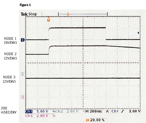
The video signal entering through connector J1 is finished, firstly, by the resistor R6 and coupled through capacitor C1 to the clamping diode D1. The clamping force sync pulses to a fixed DC level to reduce blooming effect. Potentiometer R3 is used to set the gain of the video signal, its effect is similar to the TV contrast control. The bias control (R7) is used to set the minimum level of the signal, when images are transmitted completely dark. Thus, the TV receiver can efficiently maintain synchronism. As seen below, the potentiometers R3 and R7 are adjusted together for optimal performance in all conditions.

The RF transformer T1 (and its internal capacitor) forms the tank circuit of a Hartley oscillator, which is tuned to 4.5 MHz

The audio signal that enters through J2 is coupled to the base of transistor Q3 through C2 and R4: the audio signal modulates the current at the base of Q3 to form an audio subcarrier that is higher than 4.5MHz frequency of the carrier. The modulated subcarrier frequency is applied to the modulator section through C5 and R9. The resistor R9 adjusts the level of the sub-carrier with respect to the video signal.

Transistors Q1 and Q2 amplitude modulate the audio and video signals on the RF carrier. The operating frequency is set by the coil L4, consisting of 3.5 turns of wire coating 24 on a common way with a ferrite rod. This coil is part of a Colpitts tank circuit also containing C7 and C9. The tank circuit forms a feedback network on Q4, making it oscillate at the frequency set. The RF output of the oscillator section is amplified by Q5 and Q6, whose supply voltage comes from the modulator section. The antenna adapter and low-pass filter is formed by C12, C13, and L1. The resistor R12 is optional, it is used to adapt the output to any type of antenna.

Printed Circuit:

You can use the printed circuit designed by the author, which has plenty of space for both components as well as for the battery clip, space for this subject and the island left to screw the antenna. It is possible, but make a custom PCB with minimum space required, provided that you follow the guidelines of the electrical circuit. In both cases it is advisable to use printed circuit board in place of the phenolic pertinax since the latter absorbs moisture which would cause instability of the system.

Domestic TV Transmitter PCB1

Side tracks (welding) in size. (scale 1:1)

Domestic TV Transmitter PCB

Expanded components distribution.

Notes:
  • The 4.5MHz RF transformer (T1) can be anything that fits, provided you have the internal capacitor connected to the secondary.
  • L4 must be done manually. Respect the parameters given above.
  • If used in resistor R12, to be placed on the solder side of the printed circuit between the antenna output and ground. This component must be installed whenever you use an antenna other than the internal, making a correct fit between it and the circuit.
Adjust:

To calibrate the transmitter will need a TV receiver and a signal source such as a video recorder or a camcorder. Need, moreover, a non-metallic tool to adjust the coil L4 and the transformer T1. A new 9v battery can be used for adjustments, but if calibration is difficult, try doing it with a 12v power supply. Note that during the adjustment and testing of the unit, we find that it works much better with a stable supply filtered 12 volts. If you come to the same conclusion, add a voltage input connector welding it to the appropriate points on the circuit board (instead of the battery clip).

Tune the TV receiver in an unused channel (no transmission) between 2 and 6. The TV must be connected directly to the internal antenna, an external antenna or a cable system will not work. Make sure both knobs are in the center position (at halfway) and apply power to the circuit. Adjust L4 with non-metallic tool until the TV screen goes blank (rain disappears). Then, carefully adjust L4 to achieve the best possible reception. Connect the audio outputs of a VCR and other video source to J1 and J2, if necessary operate the VCR. You should see the image on the TV screen: if so, L4 setting up the best picture possible, and if not, check the circuit board in search of an error in welds or components in the inputs. Then adjust R3 for optimum brightness and R7 for a general adjustment of video quality. You may need to make minor adjustments on L4 after adjusting R3 and R7. Finally, adjust T1 with nonmetallic tool to get the best audio possible. After that the transmitter is properly calibrated.

Domestic TV Transmitter image
View completed and mounted equipment in your cabinet

Important:

The use of these systems is regulated by law in much of the world. Before operating, we suggest that you consult a competent legal authority on the scope and restrictions of the law regarding the use of these devices. In some countries can cause illegal emissions from confiscation of equipment to the prison of the copyright holder.


read more...

5-Channel Sequencer and Two Effects

This circuit controls five 220V outputs which can be connected to each circuit of lights that will illuminate sequentially. By means of a potentiometer you can adjust the speed of movement and by means of a switch you can select the effect (one-way or round trip).

5-Channel Sequencer and Two Effects Circuit Diagram

Lights Circuit Diagram


The circuit comprises a divider by 10, a transistor oscillator stage performance and power supply. Each pulse in the integrated leg 14 rotates in the terminals (the order is: 3, 2, 4, 7, 10, 1, 5, 6, 9, 11 - in that order - and then repeat) . If a pulse is applied in the integrated leg 15 resumes from terminal 3, so that the switch I, when the bill arrives at Terminal 1 restarts and when the switch is in the I / V the count is taken complete. 4148 The ten diodes make the current integrated just go to bases and back again when going back or leg. If capacitors are placed at the bases of the transistors of values ​​that can be around 47μF (this value must be experienced) achieves a smooth effect off (dimmer) very pleasing to the eye. The higher the value of these capacitors will stay on longer and softer channel will shutdown.

Lights Circuit

CAUTION!

This circuit works with living mass, which implies a serious risk of electric shock if you touch any electrical or electronic part. Take appropriate measures to isolate ALL tracks and cables as well as triacs and sinks. Even in the oscillator transistor and the integrated there 220Vac.


read more...

Power amp (10 w) for FM Transmitter

This amplifier increases the power of an FM transmitter 50 mW to 10 W in the range 88 to 108 MHz

Power amp (10 w) for FM Transmitter Circuit Diagram

FM Transmitter Circuit Diagram

FM Transmitter


It is quite critical assembly and RF power transistors must be mounted on heat radiators and handled with utmost care.

The coil L1 is formed by 04 turns of wire of 1 mm in diameter in the form of 8 mm diameter. The coil L5 is formed of 07 turns of wire 0.5 cm in diameter in the form of 6 mm in diameter, the coil L6 is wound wire of 1 mm and consists of 03 turns in the form of 10 mm diameter. Finally coil L2 consists of 04 turns of wire of 1 mm diameter in the shape of 10 mm.

The transformer T1 includes coils L2, L3 and L4, and these coils has turns of one wire of 0.5 mm figure 2. In this same figure we have to identify the terminals of the transistors. The capacitors must be ceramic disk type or plateau and resistors are 1/4 W.


read more...

Ni-Cd Battery Charger Circuit with LM317

Today, the spread of rechargeable batteries, chargers and circuits that are required for them has led to the spread. Ni-Cd batteries, cell phones, battery-powered drills posal is widely used in many electronic devices and circuit. 

Ni-Cd Battery Charger Circuit Diagram

Battery Charger Circuit Diagram

These types of circuits are used to charge the batteries, under constant tension, provide stable current level circuits should be pretty good. The output voltage can be set for this purpose, a charging circuit is made ​​with LM317 IC regulated. Improved standard LM317'li circuit connection, the figure was obtained charging circuit.

Current limiting circuit formed by transistors, resulting high current output off, which makes the task of protecting the circuit and the batteries. Circuit, 5 Ah (Ampere-hours) of current to the battery can provide 1A'lik.

LM317 integrated circuit connected to the refrigerant heating must be avoided. Output connected batteries, charging circuit output voltage value in accordance with one or be connected in series.

read more...

4X 30W Amplifier Using TDA7386

This amplifier provides a single integrated circuit with few additional components and four independent amplifier channels to assemble a valid multichannel audio system. Based on a chip originally designed for this car audio amplifier is ideal for computers with quadraphonic sound cards like the SoundBlaster Live! Creative Labs Inc. or MosterSound Diamond Diamond Multimedia / S3.

4X 30W Amplifier Circuit Diagram

4X 30W Amplifier Circuit Diagram

As seen in the design, the only active component is the TDA7386 IC from SGS-Thomson. This provides four channels of amplification from a single source 12v. The inputs are blocked in DC from 0.1μF capacitors. The mute control terminal and stby may or may not be implemented at the discretion of the owner. The outputs are symmetrical, so that none of the speaker terminals are earthed (both are amplified).

POWER:

Since the entire system is powered by 12v decided, in our case, use a car-stereo source of armed sold and running. You can also armed one to place inside the cabinet. That is up to the owner.

HEATSINK:

Key, should be sufficient to maintain the chip in a suitable temperature. We used a Pentium III cooler with fan running. It is sufficient to connect to Vcc since 12v used as the amplifier.


read more...

20w Stereo Amplifier (2nd Revision)

This amplifier provides two channels of power up to 20 watts RMS from two line inputs. Ideal for use in computers, because its price / power / complexity is optimal. 

20w Stereo Amplifier Circuit Diagram
 
Amplifier Circuit Diagram

The drawing shows only one of the stages of the system since all circuit both stereo channels are exactly alike. Numbers in parentheses represents the equivalent of the terminal for the second channel. The heart of this project is a circuit from National Semiconductor , the LM1876 , which provides in pill two power operational amplifiers with mute function ( mute ) and standby ( off ) , which we have not implemented this design as an oversimplification .

The incoming signal , after being conditioned , level amplifier enters its non-inverting input . At the end of this part of the resulting signal is reinserted at its inverting amplifier to form the feedback network . Because the circuit is internally balanced when working with power starting not need to install the output capacitor BootStrap.en .
 
Assembly module

20w Stereo Amplifier

Mounted integrated circuit

20w Stereo Amplifier Circuit

POWER :

This system requires to operate a voltage of + / -28 Volts and a current of 2 amps. Can be used to obtain the classical source transformer , diode bridge and capacitors.

20w Stereo Amplifier Circuit Diagram

In this case the transformer should have a primary line to line voltage ( 220V) and secondary midpoint for each branch 20v ( 40v from end to end ) . The diodes should be 100V / 3A 1N5406 or equivalent type . Also usable bridge rectifier, which facilitates the task and reduces the number of tracks / space. The filter capacitors are 4700μF x 50v .
 
Picture of the power supply ( platelet )

Diagram
HEAT SINK :

All key audio system , the heatsink that this time we use is a simple cooler for Pentium III computer . We use this model since it has a surface area greater than traditional metal . To power the vast fan with taking the positive phase of the source and lower your tension with a 7812 regulator dissipated individually.


read more...

Portable and Low Power VHF FM Transmitter

This electronic circuit is a simple VHF FM transmitter circuit. The circuit can easily make portable use for a small 9 volt battery. Transmitter range from 60 to 100 meters range.  The construction of the circuit is very simple.
  • Electrically adjustable frequency between 88 and 108MHz.
  • Portable and low power consumption.
  • You can use any FM receiver.
  • 9 Volt works.
Portable and Low Power VHF FM Transmitter Circuit Diagram

FM Transmitter Circuit Diagram
Parts list:
R1 = 10K
R2 = 15K
R3 = 3.3K
R4 = 470 ohm
R5 = 100K
R6 = 4.7K
VR 1 = 10K Pot meters

VALUE
C1 = 0.1uF----- 104
C2 = 0.001uF---- 102
C3 = 0.0015uF---- 152
C4 = 10pF ----- 10
C5 = 3pfF ----- 3
C6 = 2.5pF----- 2.5
C7 = 10pF ----- 10
C8 = 0.01uF---- 103
C9 = 0.022uF----- 223
C10 = 1pF ----- 1
C11 = 0.001uF---- 102

read more...

Auto DC Motor Brake

This electronic circuit motor speed to a complete stop if you want many DC motor systems. This circuit current 1 amp 24v ranging from 6V to any DC motor, provides an automatic electronic braking. Component values ​​can be changed for some great motors.

Auto DC Motor Brake Circuit Diagram

Motor Circuit Diagram

When applied to the power circuit hobby, Q1 is turned on. These routes have zero volts gate of Q2, Q2 is closing. Diode D2 and the motor current. The power circuit is removed, the gate of Q1 Q2 C1-speed routes, some of which is stored in the load off. This is a heavy current to the motor windings providing a path for the yarn tension release Q2 turns on. R3 value, can be selected for any desired braking. Consists of zero ohm resistor R3 is fast braking time.


read more...

1-40 V, 50 mA - 5A Regulated Power Supply

Each one of the devices must counter the amateur electronics store , an adjustable voltage direct current power source. I gave the circuit diagram below 1 volt and 40 -volt power supply, the output can be adjusted arasınada as miliamperle 5 amp maximum current is adjustable from 50 .

1-40 V, 50 mA - 5A Regulated Power Supply Circuit Diagram

Regulated Power Supply Circuit Diagram

 In this way could be used for voltage source can also be used as a constant current source . Adjustable current limiting , since it is clear that the short-circuit protected . In this phase, on my testing of other circuits , and calibrations can be used successfully in conjunction with a digital voltmeter . Circuit held four transistors . Network isolation transformer , 220V primary and secondary of the power of 35 to 40 volts and 100 VA transformer should be . KBPC601 as a diode bridge ( 6A - 100V ) is sufficient. 4 6- amps instead of the bridge diode aperajlı or higher can also be used .

Half- bridge diode and 2N3005 power transitörü do KBPC601 used aluminum finned cooler isolated and connected to a profile . BD139 transistor in a small cooler plate , or use a metal box , connect the box to isolate and would be appropriate. ( I realized my extreme ısınmıyordu even when short-circuit switched connections , but as a precaution due to the cooler I'm still using a small ..) electrolytic capacitors in the circuit voltage of at least 63V Select the values ​​as I showed in the diagram . LED circuit is open or closed has no function other than to show .

The value of output voltage adjustment potentiometer is 10K . This is a linear potentiometer setting ensures that the voltage is logarithmic . Ohm resistor sets the maximum current limit of 0.5 watts or more should be 5Watt value . 500 ohm current limiting level is set by a potentiometer .

NOTE: The original version of the circuit current up to and be able to give a good cooler with a 4-5 amperes.

 However, to keep the smaller trafonuzu ( 50VA ) is sufficient for the wants and 2 amp maximum current you can change the direc 1 ohm resistance .

read more...

Electronic Combination Lock with Auto Reset


Electronic Combination Lock

Electronic Circuits Electronic Combination Lock circuit. Electronic circuit CD4013 ICs are used. 2-3-6-9 used to hold temporary password. Change the password by modifying the electronic circuit. Electronic Circuit unscheduled work. Making simple and easy. The circuit can use it anywhere you want

Electronic Combination Lock Circuit Diagram With Parts

Electronic Combination Lock Circuit Diagram

Electronic Combination Lock PCB


read more...
 
Copyright © 2019 W3circuits.blogspot.com • All Rights Reserved.
back to top